Original Link: https://www.anandtech.com/show/5261/amd-radeon-hd-7970-review
AMD Radeon HD 7970 Review: 28nm And Graphics Core Next, Together As One
by Ryan Smith on December 22, 2011 12:00 AM EST- Posted in
- AMD
- Radeon
- ATI
- Radeon HD 7000
- GPUs
While AMD and NVIDIA are consistently revising their GPU architectures, for the most part the changes they make are just that: revisions. It’s only once in a great while that a GPU architecture is thrown out entirely, which makes the arrival of a new architecture a monumental occasion in the GPU industry. The last time we saw this happen was in 2006/2007, when unified shaders and DirectX 10 lead to AMD and NVIDIA developing brand new architectures for their GPUs. Since then there have been some important revisions such as AMD’s VLIW4 architecture and NVIDIA’s Fermi architecture, but so far nothing has quite compared to 2006/2007, until now.
At AMD’s Fusion Developer Summit 2011 AMD announced Graphics Core Next, their next-generation GPU architecture. GCN would be AMD’s Fermi moment, where AMD got serious about GPU computing and finally built an architecture that would serve as both a graphics workhorse and a computing workhorse. With the ever increasing costs of high-end GPU development it’s not enough to merely develop graphics GPUs, GPU developers must expand into GPU computing in order to capture the market share they need to live well into the future.
At the same time, by canceling their 32nm process TSMC has directed a lot of hype about future GPU development onto the 28nm process, where the next generation of GPUs would be developed. In an industry accustomed to rapid change and even more rapid improvement never before have GPU developers and their buyers had to wait a full 2 years for a new fabrication process to come online.
All of this has lead to a perfect storm of anticipation for what has become the Radeon HD 7970: not only is it the first video card based on a 28nm GPU, but it’s the first member of the Southern Islands and by extension the first video card to implement GCN. As a result the Radeon HD 7970 has a tough job to fill, as a gaming card it not only needs to deliver the next-generation performance gamers expect, but as the first GCN part it needs to prove that AMD’s GCN architecture is going to make them a competitor in the GPU computing space. Can the 7970 do all of these things and live up to the anticipation? Let’s find out…


| AMD GPU Specification Comparison | ||||||
| AMD Radeon HD 7970 | AMD Radeon HD 6970 | AMD Radeon HD 6870 | AMD Radeon HD 5870 | |||
| Stream Processors | 2048 | 1536 | 1120 | 1600 | ||
| Texture Units | 128 | 96 | 56 | 80 | ||
| ROPs | 32 | 32 | 32 | 32 | ||
| Core Clock | 925MHz | 880MHz | 900MHz | 850MHz | ||
| Memory Clock | 1.375GHz (5.5GHz effective) GDDR5 | 1.375GHz (5.5GHz effective) GDDR5 | 1.05GHz (4.2GHz effective) GDDR5 | 1.2GHz (4.8GHz effective) GDDR5 | ||
| Memory Bus Width | 384-bit | 256-bit | 256-bit | 256-bit | ||
| Frame Buffer | 3GB | 2GB | 1GB | 1GB | ||
| FP64 | 1/4 | 1/4 | N/A | 1/5 | ||
| Transistor Count | 4.31B | 2.64B | 1.7B | 2.15B | ||
| Manufacturing Process | TSMC 28nm | TSMC 40nm | TSMC 40nm | TSMC 40nm | ||
| Price Point | $549 | $350 | $160 | - | ||
The Radeon HD 7970 is a card of many firsts. It’s the first video card using a 28nm GPU. It’s the first card supporting Direct3D 11.1. It’s the first member of AMD’s new Southern Islands Family. And it’s the first video card implementing AMD’s Graphics Core Next architecture. All of these attributes combine to make the 7970 quite a different video card from any AMD video card before it.
Cutting right to the chase, the 7970 will serve as AMD’s flagship video card for the Southern Islands family. Based on a complete AMD Tahiti GPU, it has 2048 stream processors organized according to AMD’s new SIMD-based GCN architecture. With so many stream processors coupled with a 384bit GDDR5 memory bus, it’s no surprise that Tahiti is has the highest transistor count of any GPU yet: 4.31B transistors. Fabricated on TSMC’s new 28nm High-K process, this gives it a die size of 365mm2, making it only slightly smaller than AMD’s 40nm Cayman GPU at 389mm2.
Looking at specifications specific to the 7970, AMD will be clocking it at 925MHz, giving it 3.79TFLOPs of theoretical computing performance compared to 2.7TFLOPs under the much different VLIW4 architecture of the 6970. Meanwhile the wider 384bit GDDR5 memory bus for 7970 will be clocked at 1.375GHz (5.5GHz data rate), giving it 264GB/sec of memory bandwidth, a significant jump over the 176GB/sec of the 6970.
These functional units are joined by a number of other elements, including 8 ROP partitions that can process 32 ROPs per clock, 128 texture units divided up among 32 Compute Units (CUs), and a fixed function pipeline that contains a pair of AMD’s 9th generation geometry engines. Of course all of this hardware would normally take quite a bit of power to run, but thankfully power usage is kept in check by the advancements offered by TSMC’s 28nm process. AMD hasn’t provided us with an official typical board power, but we estimate it’s around 220W, with an absolute 250W PowerTune limit. Meanwhile idle power usage is looking particularly good, as thanks to AMD's further work on power savings their typical power consumption under idle is only 15W. And with AMD's new ZeroCore Power technology (more on that in a bit), idle power usage drops to an asbolutely miniscule 3W.
Overall for those of you looking for a quick summary of performance, the 7970 is quite powerful, but it may not be as powerful as you were expecting. Depending on the game being tested it’s anywhere between 5% and 35% faster than NVIDIA’s GeForce GTX 580, averaging 15% to 25% depending on the specific resolution in use. Furthermore thanks to TSMC’s 28nm process power usage is upwards of 50W lower than the GTX 580, but it’s still higher than the 6970 it replaces. As far as performance jumps go from new fabrication processes, this isn’t as big a leap as we’ve seen in the past.
In a significant departure from the launch of the Radeon HD 5870 and 4870, AMD will not be pricing the 7970 nearly as aggressively as those cards with its launch. The MSRP for the 7970 will be $550, a premium price befitting a premium card, but a price based almost exclusively on the competition (e.g. the GTX 580) rather than one that takes advantage of cheaper manufacturing costs to aggressively undercuts the competition. In time AMD needs to bring down the price of the card, but for the time being they will be charging a price premium reflecting the card’s status as the single-GPU king.
For those of you trying to decide whether to get a 7970, you will have some time to decide. This is a soft launch; AMD will not make the 7970 available until January 9th (the day before the Consumer Electronics Show), nearly 3 weeks from now. We don’t have any idea what the launch quantities will be like, but from what we hear TSMC’s 28nm process has finally reached reasonable yields, so AMD should be in a better position than the 5870 launch. The price premium on the card will also help taper demand side some, though even at $550 this won’t rule out the first batch of cards selling out.
Beyond January 9th, AMD as an entire family of Southern Islands video cards still to launch. AMD will reveal more about those in due time, but as with the Evergreen and Northern Islands families AMD has a plan to introduce a number of video cards over the next year. So 7970 is just the beginning.
| Winter 2011 GPU Pricing Comparison | |||||
| AMD | Price | NVIDIA | |||
| $750 | GeForce GTX 590 | ||||
| Radeon HD 6990 | $700 | ||||
| Radeon HD 7970 | $549 | ||||
| $500 | GeForce GTX 580 | ||||
| Radeon HD 6970 | $350 | GeForce GTX 570 | |||
| Radeon HD 6950 2GB | $250 | ||||
| $240 | GeForce GTX 560 Ti | ||||
| Radeon HD 6870 | $160 | ||||
A Quick Refresher: Graphics Core Next
One of the things we’ve seen as a result of the shift from pure graphics GPUs to mixed graphics and compute GPUs is how NVIDIA and AMD go about making their announcements and courting developers. With graphics GPUs there was no great need to discuss products or architectures ahead of time; a few choice developers would get engineering sample hardware a few months early, and everyone else would wait for the actual product launch. With the inclusion of compute capabilities however comes the need to approach launches in a different manner, a more CPU-like manner.
As a result both NVIDIA and AMD have begun revealing their architectures to developers roughly six months before the first products launch. This is very similar to how CPU launches are handled, where the basic principles of an architecture are publically disclosed months in advance. All of this is necessary as the compute (and specifically, HPC) development pipeline is far more focused on optimizing code around a specific architecture in order to maximize performance; whereas graphics development is still fairly abstracted by APIs, compute developers want to get down and dirty, and to do that they need to know as much about new architectures as possible as soon as possible.
It’s for these reasons that AMD announced Graphics Core Next, the fundamental architecture behind AMD’s new GPUs, back in June of this year at the AMD Fusion Developers Summit. There are some implementation and product specific details that we haven’t known until now, and of course very little was revealed about GCN’s graphics capabilities, but otherwise on the compute side AMD is delivering on exactly what they promised 6 months ago.
Since we’ve already covered the fundamentals of GCN in our GCN preview and the Radeon HD 7970 is primarily a gaming product we’re not going to go over GCN in depth here, but I’d encourage you to read our preview to fully understand the intricacies of GCN. But if you’re not interested in that, here’s a quick refresher on GCN with details pertinent to the 7970.
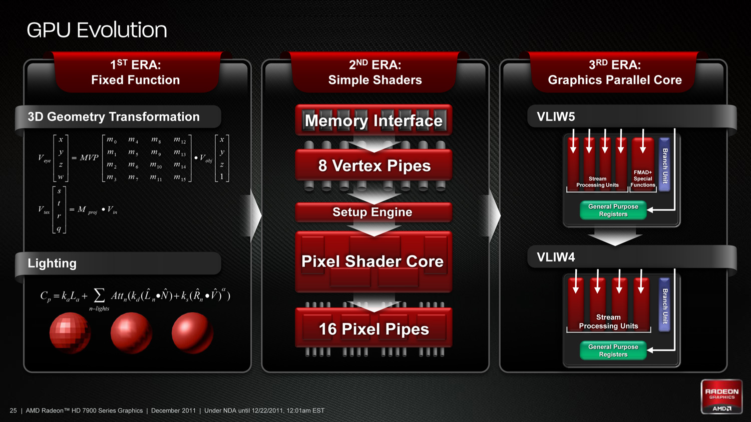
As we’ve already seen in some depth with the Radeon HD 6970, VLIW architectures are very good for graphics work, but they’re poor for compute work. VLIW designs excel in high instruction level parallelism (ILP) use cases, which graphics falls under quite nicely thanks to the fact that with most operations pixels and the color component channels of pixels are independently addressable datum. In fact at the time of the Cayman launch AMD found that the average slot utilization factor for shader programs on their VLIW5 architecture was 3.4 out of 5, reflecting the fact that most shader operations were operating on pixels or other data types that could be scheduled together
Meanwhile, at a hardware level VLIW is a unique design in that it’s the epitome of the “more is better” philosophy. AMD’s high steam processor counts with VLIW4 and VLIW5 are a result of VLIW being a very thin type of architecture that purposely uses many simple ALUs, as opposed to fewer complex units (e.g. Fermi). Furthermore all of the scheduling for VLIW is done in advance by the compiler, so VLIW designs are in effect very dense collections of simple ALUs and cache.
The hardware traits of VLIW mean that for a VLIW architecture to work, the workloads need to map well to the architecture. Complex operations that the simple ALUs can’t handle are bad for VLIW, as are instructions that aren’t trivial to schedule together due to dependencies or other conflicts. As we’ve seen graphics operations do map well to VLIW, which is why VLIW has been in use since the earliest pixel shader equipped GPUs. Yet even then graphics operations don’t achieve perfect utilization under VLIW, but that’s okay because VLIW designs are so dense that it’s not a big problem if they’re operating at under full efficiency.
When it comes to compute workloads however, the idiosyncrasies of VLIW start to become a problem. “Compute” covers a wide range of workloads and algorithms; graphics algorithms may be rigidly defined, but compute workloads can be virtually anything. On the one hand there are compute workloads such as password hashing that are every bit as embarrassingly parallel as graphics workloads are, meaning these map well to existing VLIW architectures. On the other hand there are tasks like texture decompression which are parallel but not embarrassingly so, which means they map poorly to VLIW architectures. At one extreme you have a highly parallel workload, and at the other you have an almost serial workload.
Cayman, A VLIW4 Design
So long as you only want to handle the highly parallel workloads VLIW is fine. But using VLIW as the basis of a compute architecture is going is limit what tasks your processor is sufficiently good at. If you want to handle a wider spectrum of compute workloads you need a more general purpose architecture, and this is the situation AMD faced.
But why does AMD want to chase compute in the first place when they already have a successful graphics GPU business? In the long term GCN plays a big part in AMD’s Fusion plans, but in the short term there’s a much simpler answer: because they have to.
In Q3’2011 NVIDIA’s Professional Solutions Business (Quadro + Tesla) had an operating income of 95M on 230M in revenue. Their (consumer) GPU business had an operating income of 146M, but on a much larger 644M in revenue. Professional products have much higher profit margins and it’s a growing business, particularly the GPU computing side. As it stands NVIDIA and AMD may have relatively equal shares of the discrete GPU market, but it’s NVIDIA that makes all the money. For AMD’s GPU business it’s no longer enough to focus only on graphics, they need a larger piece of the professional product market to survive and thrive in the future. And thus we have GCN.
A Quick Refresher, Cont
Having established what’s bad about VLIW as a compute architecture, let’s discuss what makes a good compute architecture. The most fundamental aspect of compute is that developers want stable and predictable performance, something that VLIW didn’t lend itself to because it was dependency limited. Architectures that can’t work around dependencies will see their performance vary due to those dependencies. Consequently, if you want an architecture with stable performance that’s going to be good for compute workloads then you want an architecture that isn’t impacted by dependencies.
Ultimately dependencies and ILP go hand-in-hand. If you can extract ILP from a workload, then your architecture is by definition bursty. An architecture that can’t extract ILP may not be able to achieve the same level of peak performance, but it will not burst and hence it will be more consistent. This is the guiding principle behind NVIDIA’s Fermi architecture; GF100/GF110 have no ability to extract ILP, and developers love it for that reason.
So with those design goals in mind, let’s talk GCN.
VLIW is a traditional and well proven design for parallel processing. But it is not the only traditional and well proven design for parallel processing. For GCN AMD will be replacing VLIW with what’s fundamentally a Single Instruction Multiple Data (SIMD) vector architecture (note: technically VLIW is a subset of SIMD, but for the purposes of this refresher we’re considering them to be different).
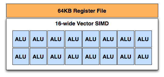
A Single GCN SIMD
At the most fundamental level AMD is still using simple ALUs, just like Cayman before it. In GCN these ALUs are organized into a single SIMD unit, the smallest unit of work for GCN. A SIMD is composed of 16 of these ALUs, along with a 64KB register file for the SIMDs to keep data in.
Above the individual SIMD we have a Compute Unit, the smallest fully independent functional unit. A CU is composed of 4 SIMD units, a hardware scheduler, a branch unit, L1 cache, a local date share, 4 texture units (each with 4 texture fetch load/store units), and a special scalar unit. The scalar unit is responsible for all of the arithmetic operations the simple ALUs can’t do or won’t do efficiently, such as conditional statements (if/then) and transcendental operations.
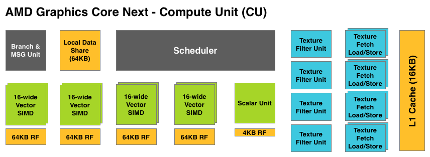
Because the smallest unit of work is the SIMD and a CU has 4 SIMDs, a CU works on 4 different wavefronts at once. As wavefronts are still 64 operations wide, each cycle a SIMD will complete ¼ of the operations on their respective wavefront, and after 4 cycles the current instruction for the active wavefront is completed.
Cayman by comparison would attempt to execute multiple instructions from the same wavefront in parallel, rather than executing a single instruction from multiple wavefronts. This is where Cayman got bursty – if the instructions were in any way dependent, Cayman would have to let some of its ALUs go idle. GCN on the other hand does not face this issue, because each SIMD handles single instructions from different wavefronts they are in no way attempting to take advantage of ILP, and their performance will be very consistent.
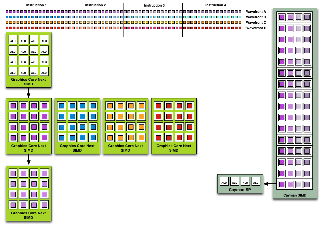
Wavefront Execution Example: SIMD vs. VLIW. Not To Scale - Wavefront Size 16
There are other aspects of GCN that influence its performance – the scalar unit plays a huge part – but in comparison to Cayman, this is the single biggest difference. By not taking advantage of ILP, but instead taking advantage of Thread Level Parallism (TLP) in the form of executing more wavefronts at once, GCN will be able to deliver high compute performance and to do so consistently.
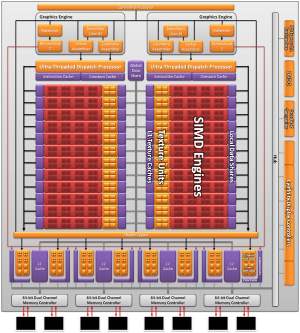
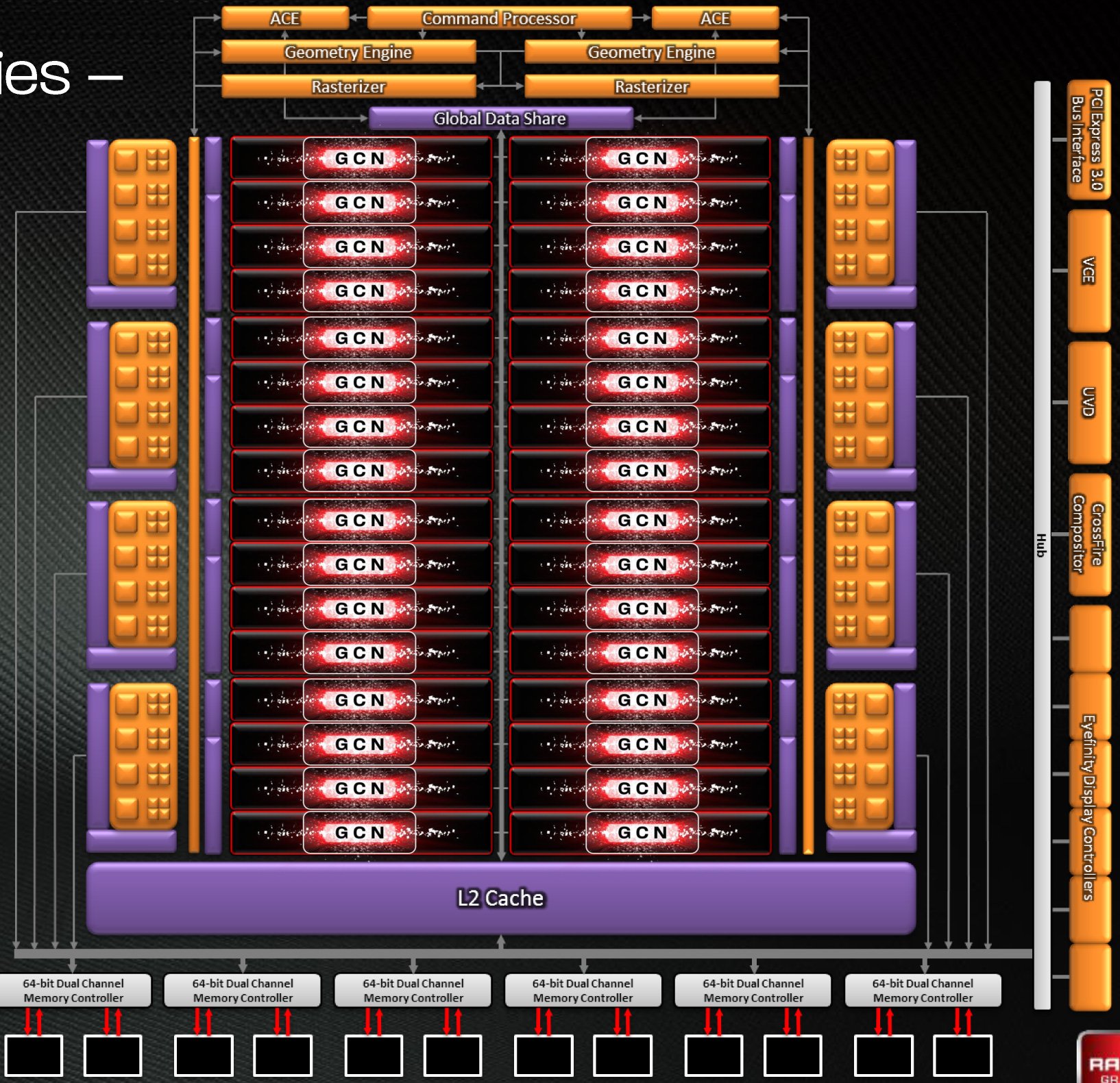
Bringing this all together, to make a complete GPU a number of these GCN CUs will be combined with the rest of the parts we’re accustomed to seeing on a GPU. A frontend is responsible for feeding the GPU, as it contains both the command processors (ACEs) responsible for feeding the CUs and the geometry engines responsible for geometry setup. Meanwhile coming after the CUs will be the ROPs that handle the actual render operations, the L2 cache, the memory controllers, and the various fixed function controllers such as the display controllers, PCIe bus controllers, Universal Video Decoder, and Video Codec Engine.
At the end of the day if AMD has done their homework GCN should significantly improve compute performance relative to VLIW4 while gaming performance should be just as good. Gaming shader operations will execute across the CUs in a much different manner than they did across VLIW, but they should do so at a similar speed. And for games that use compute shaders, they should directly benefit from the compute improvements. It’s by building out a GPU in this manner that AMD can make an architecture that’s significantly better at compute without sacrificing gaming performance, and this is why the resulting GCN architecture is balanced for both compute and graphics.
Building Tahiti & The Southern Islands
Now that we’ve had a chance to go over the basis of the Graphics Core Next architecture, let’s talk about the finished products.
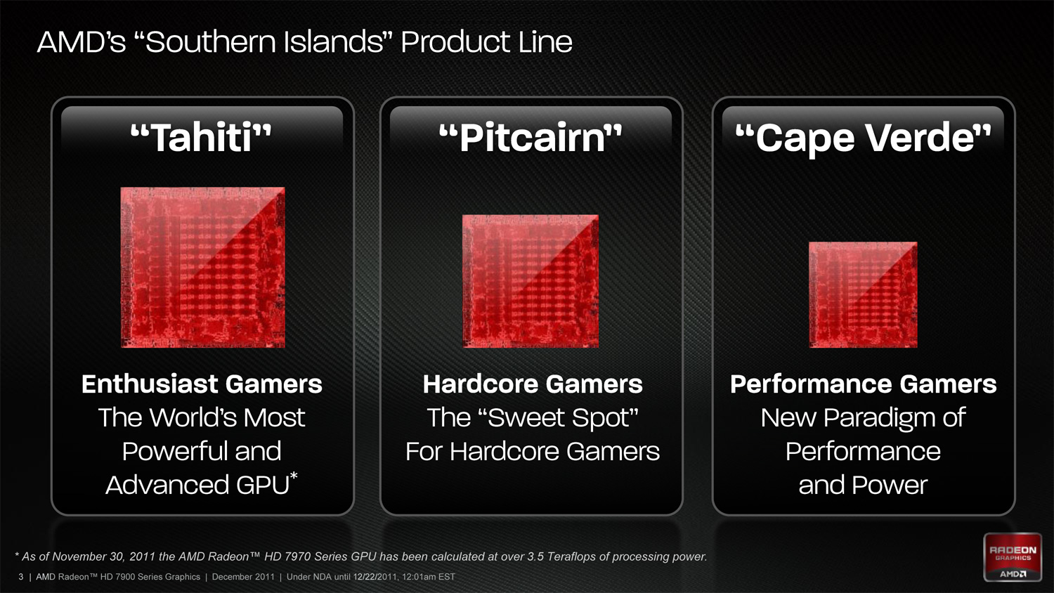
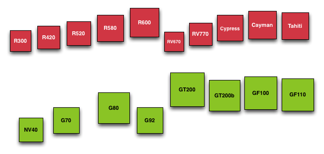
Today AMD will be launching Tahiti, the first GPU of the Southern Islands family. Southern Islands will initially be composed of 3 GPUs: Tahiti, Pitcairn, and Cape Verde. Tahiti is the largest and most powerful member of the Southern Islands family, while Pitcairn and Cape Verde get progressively smaller. AMD has not yet announced the branding or launch dates for Pitcarn and Cape Verde, but it typically takes AMD around 6 months to launch a complete family. As such it’s reasonable to expect that all 3 GPUs will have launched by the end of June although there’s a good likelihood of it happening sooner than that.
All 3 GPUs are based on the GCN architecture, and as family members will have similar features while varying the number of functional units accordingly. Along with the architecture change Southern Islands brings with it a slew of additional features that we’ll get to in the following pages, including Partially Resident Texture (PRT) support, PCIe 3.0, FastHDMI, Direct3D 11.1, and AMD’s fixed-function H.264 encoder, the Video Codec Engine.
But today is all about Tahiti, so let’s get down to business.
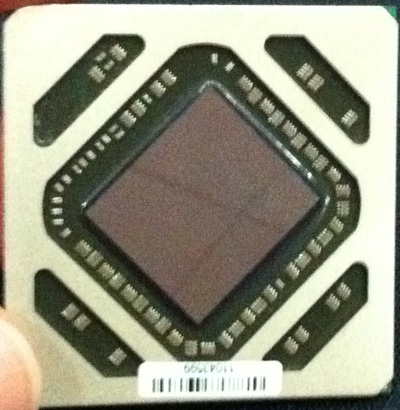
As we quickly covered in our introduction, Tahiti is a 4.31B transistor GPU based on the GCN architecture and built on TSMC’s new 28nm High-K process. Due to TSMC canceling their 32nm process last year AMD has had to wait over 2 years for the next full node rather than taking advantage of the half-node process as they typically do, and as a result the jump from Cayman at 40nm to Tahiti at 28nm is much bigger than with past product launches. Whereas Cayman had 2.64B transistors and a die size of 389mm2, Tahiti has a whopping 63% more transistors than Cayman and yet it’s still smaller, coming in at a slightly more petite 365mm2.
GPU Die Size Comparison
At this point AMD hasn’t provided us with the typical board power values for 7970, but we do know that PowerTune is limited to 250W. In terms of design 7970 is clearly intended to work in similar environments as the 6970, in which case power consumption should be similar to the 6970.
Interestingly enough however we’re hearing that 7970 cards are proving to be very overclockable, which is a good sign for the state of TSMC’s 28nm process, and at the same time a bit distressing. Moore’s Law has continued to hold with respect to transistor density, but the power consumption benefits of using smaller nodes has continued to wane. Having a lot of overclocking headroom means that the 7970 has the potential to be much faster, but it also means that the 7970 (and 28nm GPUs in general) are going to be bottlenecked by power. In which case seeing as how we’re already approaching 300W with single-GPU video cards, the performance gains realized from future fabrication processes would be limited to the ever diminishing returns on power consumption improvements.
Diving deeper into Tahiti, as per the GCN architecture Tahiti’s 2048 SPs are organized into 32 Compute Units. Each of these CUs contains 4 texture units and 4 SIMD units, along with a scalar unit and the appropriate cache and registers. At the 7970’s core clock of 925MHz this puts Tahiti’s theoretical FP32 compute performance at 3.79TFLOPs, while its FP64 performance is ¼ that at 947GFLOPs. As GCN’s FP64 performance can be configured for 1/16, ¼, or ½ its FP32 performance it’s not clear at this time whether the 7970’s ¼ rate was a hardware design decision for Tahiti or a software cap that’s specific to the 7970. However as it’s obvious that Tahiti is destined to end up in a FireStream card we will no doubt find out soon enough.
Meanwhile the frontend/command processor for Tahiti is composed of 2 Asynchronous Command Engines (ACEs) and 2 geometry engines. Just as with Cayman each geometry engine can dispatch 1 triangle per clock, giving Tahiti the same theoretical 2 triangle/clock rate as Cayman. As we’ll see however, in practice Tahiti will be much faster than Cayman here due to efficiency improvements.
Looking beyond the frontend and shader cores, we’ve seen a very interesting reorganization of the rest of the GPU as opposed to Cayman. Keeping in mind that AMD’s diagrams are logical diagrams rather than physical diagrams, the fact that the ROPs on Tahiti are not located near the L2 cache and memory controllers in the diagram is not an error. The ROPs have in fact been partially decoupled from the L2 cache and memory controllers, which is also why there are 8 ROP partitions but only 6 memory controllers. Traditionally the ROPs, L2 cache, and memory controllers have all been tightly integrated as ROP operations are extremely bandwidth intensive, making this a very unusual design for AMD to use.
As it turns out, there’s a very good reason that AMD went this route. ROP operations are extremely bandwidth intensive, so much so that even when pairing up ROPs with memory controllers, the ROPs are often still starved of memory bandwidth. With Cayman AMD was not able to reach their peak theoretical ROP throughput even in synthetic tests, never mind in real-world usage. With Tahiti AMD would need to improve their ROP throughput one way or another to keep pace with future games, but because of the low efficiency of their existing ROPs they didn’t need to add any more ROP hardware, they merely needed to improve the efficiency of what they already had.
The solution to that was rather counter-intuitive: decouple the ROPs from the memory controllers. By servicing the ROPs through a crossbar AMD can hold the number of ROPs constant at 32 while increasing the width of the memory bus by 50%. The end result is that the same number of ROPs perform better by having access to the additional bandwidth they need.
The big question right now, and one we don’t have an answer to, is what were the tradeoffs for decoupling the ROPs? Clearly the crossbar design has improved ROP performance through the amount of memory bandwidth they can access, but did it impact anything else? The most obvious tradeoff here would be for potentially higher latency, but there may be other aspects that we haven’t realized yet.
On that note, let’s discuss the memory controllers quickly. Tahiti’s memory controllers aren’t significantly different from Cayman’s but there are more of them, 50% more in fact, forming a 384bit memory bus. AMD has long shied away from non-power of 2 memory busses, and indeed the last time they even had a memory bus bigger than 256bits was with the ill-fated 2900XT, but at this point in time AMD has already nearly reached the practical limits of GDDR5. AMD’s ROPs needed more memory bandwidth, but even more than that AMD needed more memory bandwidth to ensure Tahiti had competitive compute performance, and as such they had little choice but to widen their memory bus to 384bits wide by adding another 2 memory controllers.
It’s worth noting though that the addition of 2 more memory controllers also improves AMD’s cache situation. With 128KB of L2 cache being tied to each memory controller, the additional controllers gave AMD 768KB of L2 cache, rather than the 512KB that a 256bit memory bus would be paired with.
Tahiti: The First Direct3D 11.1 GPU
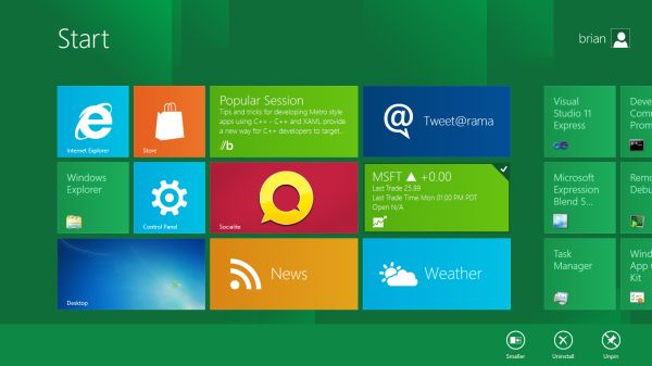
One of the many changes coming in Windows 8 next year will be the next iteration of Direct3D, which will be Direct3D 11.1. More so than any other version of Direct3D so far, D3D11.1 is best summed up as a housekeeping release. There will be some new features, but compared to even past point releases such as 10.1 and 9c it’s a small release that’s going to be focusing more on improving the API itself – particularly interoperability with SoC GPUs for Windows 8 – than it will be about introducing new features. This is largely a consequence of the growing length of time for all matters of development hardware and software. By the time Windows 8 ships Direct3D 11 will be 3 years old, but these days that’s shorter than the development period for some AAA games. Direct3D 11/11.1 will continue to be the current Windows 3D API for quite some time to come.
With regards to backward compatibility in D3D11.1, there’s one new feature in particular that requires new hardware to support it: Target Independent Rasterization. As a result AMD’s existing D3D11 GPUs cannot fully support D3D11.1, thereby making Tahiti the first D3D 11.1 GPU to be released. In practice this means that the hardware is once again ahead of the API, even more so than what we saw with G80 + D3D10 or Cypress (5870) + D3D11 since D3D11.1 isn’t due to arrive for roughly another year. For the time being Tahiti’s hardware supports it but AMD won’t enable this functionality until the future – the first driver with D3D11.1 support will be a beta driver for Windows 8, which we expect we’ll see for the Windows 8 beta next year.
So what does D3D11.1 bring to the table? The biggest end user feature is going to be the formalization of Stereo 3D support into the D3D API. Currently S3D is achieved by either partially going around D3D to present a quad buffer to games and applications that directly support S3D, or in the case of driver/middleware enhancement manipulating the rendering process itself to get the desired results. Formalizing S3D won’t remove the need for middleware to enable S3D on games that choose not to implement it, but for games that do choose to directly implement it such as Deus Ex, it will now be possible to do this through Direct3D.
S3D related sales have never been particularly spectacular, and no doubt the fragmentation of the market is partially to blame, so this may be the push in the right direction that the S3D market needs, if the wider consumer base is ready to accept it. At a minimum this should remove the need for any fragmentation/customization when it comes to games that directly support S3D.
With S3D out of the way, the rest of the D3D11.1 feature set isn’t going to be nearly as visible. Interoperability between graphics, video, and compute is going to be greatly improved, allowing video via Media Foundation to be sent through pixel and compute shaders, among other things. Meanwhile target independent rasterization and some new buffer commands should give developers a few more tricks to work with, while double precision (FP64) support will be coming to pixel shaders on hardware that has FP64 support.
Finally, looking at things at a lower level D3D11.1 will be released alongside DXGI 1.2 and WDDM 1.2, the full combination of which will continue Microsoft’s long-term goal of making the GPU more CPU-like. One of Microsoft’s goals has to been to push GPU manufacturers to improve the granularity of GPU preemption, both for performance and reliability purposes. Since XP things have gotten better as Vista introduced GPU Timeout Detection and Recovery (TDR) to reset hung GPUs, and a finer level of granularity has been introduced to allow multiple games/applications to share a GPU without stomping all over each other, but preemption and context switches are still expensive on a GPU compared to a CPU (there are a lot of registers to deal with) which impacts performance and reliability.
To that end preemption is being given a bit more attention, as WDDM 1.2 will be introducing some new API commands to help manage it while encouraging hardware developers to support finer grained preemption. Meanwhile to improve reliability TDR is getting a major addition by being able to do a finer grained reset of the GPU. Currently with Windows 7 a TDR triggers a complete GPU reset, but with Windows 8 and WDDM 1.2 the GPU will be compartmentalized into “engines” that can be individually reset. Only the games/applications using a reset engine will be impacted while everything else is left untouched, and while most games and applications can already gracefully handle a reset, this will further reduce the problems a reset creates by resetting fewer programs.
Partially Resident Textures: Not Your Father’s Megatexture
John Carmack’s id Software may not be the engine licensing powerhouse it was back in the Quake 3 days, but that hasn’t changed the revolutionary nature of his engine designs. The reason we bring this up is because there’s a great deal of GPU technology that can be directly mapped to concepts Carmack first implemented. For id Tech 4 Carmack implemented shadow volume technology, which was then first implemented in hardware by NVIDIA as their UltraShadow technology, and has since then been implemented in a number of GPUs. For id Tech 5 the trend has continued, now with AMD doing a hardware implementation of a Carmack inspired technology.
Among the features added to Graphics Core Next that were explicitly for gaming, the final feature was Partially Resident Textures, which many of you are probably more familiar with in concept as Carmack’s MegaTexture technology. The concept behind PRT/Megatexture is that rather than being treated as singular entities, due to their size textures should be broken down into smaller tiles, and then the tiles can be used as necessary. If a complete texture isn’t needed, then rather than loading the entire texture only the relevant tiles can be loaded while the irrelevant tiles can be skipped or loaded at a low quality. Ultimately this technology is designed to improve texture streaming by streaming tiles instead of whole textures, reducing the amount of unnecessary texture data that is streamed.
Currently MegaTexture does this entirely in software using existing OpenGL 3.2 APIs, but AMD believes that more next-generation game engines will use this type of texturing technology. Which makes it something worth targeting, as if they can implement it faster in hardware and get developers to use it, then it will improve game performance on their cards. Again this is similar to volume shadows, where hardware implementations sped up the process.
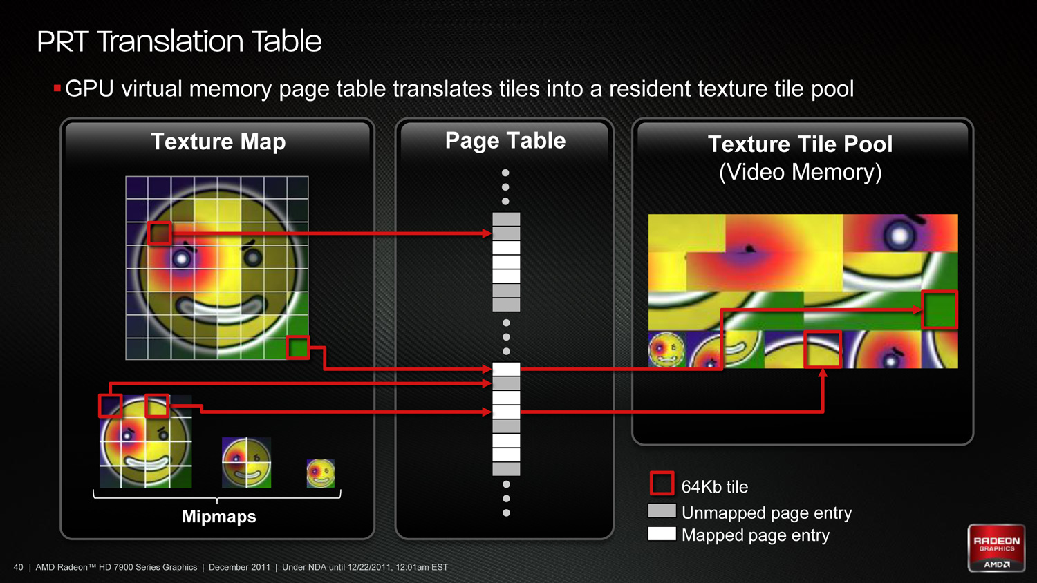
In order to implement this in hardware AMD has to handle two things: texture conversion, and cache management. With texture conversion, textures need to be read and broken up into tiles; AMD is going with a texture format agnostic method here that can simply chunk textures as they stand, keeping the resulting tiles in the same format. For AMD’s technology each tile will be 64KB, which for an uncompressed 32bit texture would be enough room for a 128 x 128 chunk.
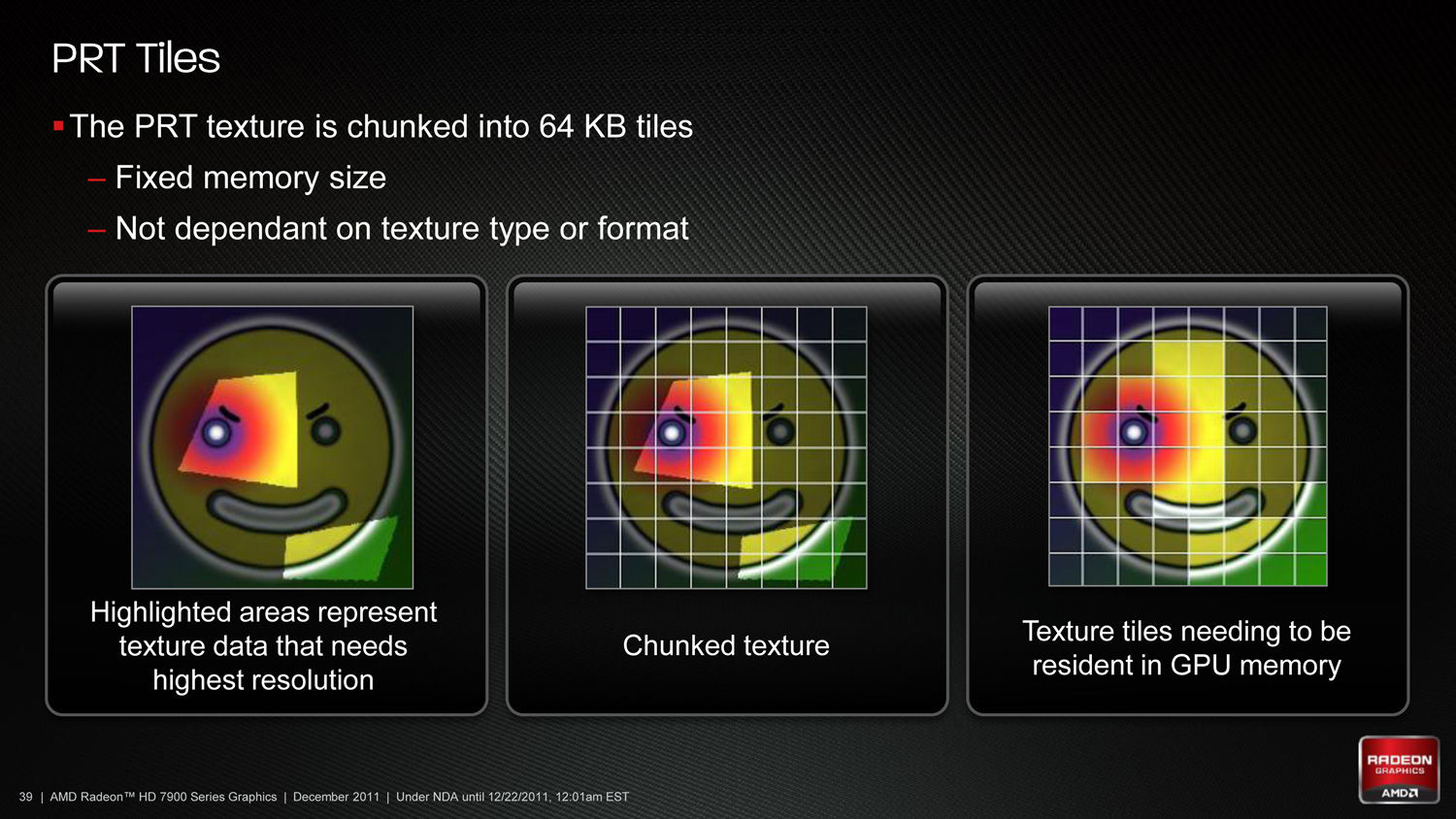
The second aspect of PRT is managing the tiles. In essence PRT reduces local video memory to a very large cache, where tiles are mapped/pinned as necessary and then evicted as per the cache rules, and elsewhere the hardware handles page/tile translation should a tile not already be in the cache. Large tomes have been written on caching methods, and this aspect is of particular interest to AMD because what they learn about caching here they can apply to graphical workloads (i.e. professional) and not just gaming.
To that end AMD put together a technology demo for PRT based on Per-Face Texture Mapping (PTEX), a Disney-developed texture mapping technique that maps textures to polygons in a 1:1 ratio. Disney uses this technique for production rendering, as by constraining textures to a single polygon they don’t have to deal with any complexities that arise as a result of mapping a texture over multiple polygons. In the case of AMD’s demo it not only benefits for the reasons that Disney uses it, but also because when combined with tessellation it trivializes vector displacement, making art generation for tessellated games much easier to create. Finally, PRT fits into all of this by improving the efficiency of accessing and storing the Ptex texture chunks.
Wrapping things up, for the time being while Southern Islands will bring hardware support for PRT software support will remain limited. As D3D is not normally extensible it’s really only possible to easily access the feature from other APIs (e.g. OpenGL), which when it comes to games is going to greatly limit the adoption of the technology. AMD of course is working on the issue, but there are few ways around D3D’s tight restrictions on non-standard features.


Display Tech: HD3D Eyefinity, MST Hubs, & DDM Audio
With the launch of the HD 5000 series back in 2009 AMD managed to get the drop on everyone, press and NVIDIA alike. Eyefinity, AMD’s Single Large Surface technology, came out of virtually nowhere thanks to a carefully orchestrated development plan that ensured very few people even within AMD knew about it. As a result of everything that was leaked ahead of time Eyefinity was not, making it AMD’s big eye catcher for the 5000 series.
As what was to be the first piece of the much dreamed about holodeck, AMD has been steadily working on it since 2009 in order to improve the experience even within their existing hardware by adding support for such features as bezel compensation and combining CrossFire with Eyefinity. For AMD it’s a feature of great importance even if end user adoption is still limited.
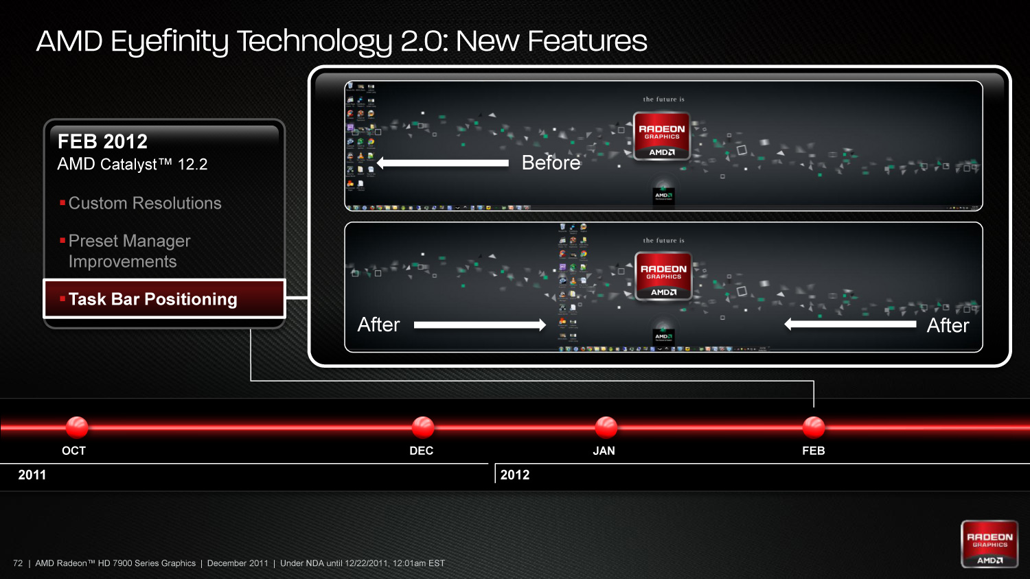
For the Southern Islands family AMD isn’t going to be pulling quite the rabbit out of their hat this time when it comes to displays. Southern Islands’ new display feature will be Discrete Digital Multi-Point Audio (which we’ll get to in a moment), but this doesn’t mean that AMD hasn’t continued to work on Eyefinity. Since October AMD has been engaged in an initiative they’re calling “Eyefinity Technology 2.0”, which is going to be pushed as a big part of the Southern Islands launch even though these are software improvements that will benefit all cards.
So what is Eyefinity Technology 2.0 composed of? We’ve already seen several new features starting with Catalyst 11.10, such as 5x1 portrait and landscape support and flexible bezel compensation support. The next step is going to be integrating Stereo 3D (or as AMD likes to call it, HD3D) into the mix, similar to how NVIDIA has 3D Vision Surround. Catalyst 11.12 introduced the ability to use HD3D with an Eyefinity display setup, and Catalyst 12.1 (preview out now) added support to do that in a CrossFire configuration. The final step is going to be with Catalyst 12.2 in February, which will add support for custom resolutions and the ability to relocate the Windows task bar to an arbitrary screen, two features that users have been asking about for quite some time. Again, all of these improvements are driver side, but they are a major component of AMD’s marketing for Southern Islands.
Speaking about Eyefinity, one issue that comes up time and time again is Multi Stream Transport (MST) hubs. We were introduced to MST hubs back with the launch of the 6800 series, which allowed a single DP 1.2 port to drive up to 4 monitors by taking advantage of the high bandwidth of DP1.2 and embedding transport streams for several monitors into the signal. The purpose of MST hubs was so that users could use several monitors with a regular Radeon card, rather than needing an exotic all-DisplayPort “Eyefinity edition” card as they need now.
But as many of you have asked me about, several deadlines for MST hubs have come and gone, including the latest deadline which was supposed to be by the end of this year. As with active DP adaptors this is largely out of AMD’s hands since they don’t produce the hardware, but they have been continuing to prod their partners on the issue. The latest deadline from AMD isn’t rosy – summer of 2012 – but they seem more confident of this deadline than deadlines in the past. Not that another half-year wait will be of any comfort for users who have been looking for MST hubs for the better part of the year, but at least it provides some idea on when to expect them.
Last, but certainly not least on the display technologies front is AMD’s new feature for Southern Islands, Discrete Digital Multi-Point Audio (DDMA). It’s a mouthful of a name but the concept is rather simple: it’s the next step in audio output from a video card. Video cards have been able to output audio for a few years now via HDMI, and more recently DisplayPort gained the ability. However GPUs have been limited to streaming audio to a single device, be it a monitor, TV, or receiver. With DDMA GPUs can send audio to multiple devices, and AMD is looking at how to put that ability to work.

The most basic use for being able to send audio to multiple devices is to individually address the speakers of each device, which is the cornerstone of AMD’s proposed use cases. Fundamentally AMD is looking at applications that involve matching audio streams to the monitor the relevant application is on – move a video player from your center monitor to your left monitor, and the audio from that video player should also move from the speakers on the middle monitor to the speakers on the left monitor. What can you do with speakers that are mapped to monitors? That’s what AMD wants to find out.
Being realistic for a moment, the 7970 isn’t going to be the card that sells this feature, as it’s a $550 gamer video card. Gamers are using dedicated 2.1/5.1/7.1 audio systems or headphones for surround sound, and while AMD does have a proposed multi-tasking use case for this it’s not very convincing. DDMA will become much more important on future lower end cards as those are the cards that go into family desktops, workstations, and the like. Thus the killer app for this feature (and certainly AMD’s best prepared scenario) is for video conferencing where each attendee is mapped to a monitor, and with DDMA a set of speakers on that monitor. AMD’s partner Oovoo is working on just such a system though it’s still early in development.
Display Tech, Cont: Fast HDMI
Moving on from multi-monitor applications, AMD has not only been working on technologies for multi-monitor users. Southern Islands will also include some video and movie technologies that will be relevant for single and multi-monitor uses alike.
With the 6000 series AMD upgraded their DisplayPort capabilities from DP 1.1 to DP 1.2. With Southern Islands AMD will be upgrading their HDMI capabilities. Currently AMD supports a subset of the complete HDMI 1.4a specification; they can drive S3D displays (the killer feature of 1.4a), but that’s the only thing out of 1.4a they support. HDMI also introduced support for 4K x 2K displays, but both displays and devices that can drive them have been rare. As displays start to become available so too does support for them with AMD’s products.
As per the relevant specifications, both DP 1.2 and HDMI 1.4a can drive 4K x 2K displays, but with the 6000 series the hardware could only handle such a display over DP 1.2. With HDMI it was an issue of bandwidth, as HDMI is based on DVI and uses the same TMDS signaling technology. At normal speed HDMI only has as much bandwidth as single-link HDMI (~4Gbps) which is not enough to drive such a large display. DVI solved this with dual-link DVI, whereas as of HDMI 1.3 the HDMI consortium solved this by tightening their cable specifications to allow for higher clocked transmissions, from 165MHz up to 340MHz.

It’s this higher transmission speed that AMD is adding support for in Southern Islands. AMD calls this Fast HDMI technology, which as near as we can tell is not any kind of HDMI trademark but simply AMD’s branding for high speed HDMI. With Fast HDMI AMD will be able to drive 4K x 2K displays over HDMI – which looks like it will be the common connector for TVs at those high resolutions – along with being able to support 1080P S3D at higher framerates with next-generation TVs. Currently AMD’s cards and TVs alike can only handle 1080P frame packed S3D at up to 48fps (24Hz/eye), or with a bit of hacking up to 60fps (30Hz/eye), which is fine for 24fps movies but much too low for gaming. As next-generation TVs add support for 1080P frame packed S3D at 120fps (60Hz/eye) Southern Islands products will be the first AMD products able to drive them over HDMI through the use of Fast HDMI.
The only remaining questions at this point are just how high does AMD’s Fast HDMI clock (they don’t necessary have to hit 340MHz), and if AMD will add support for any other features that higher bandwidths enable. AMD says that Southern Islands supports “3GHz HDMI”, which appears to be a misnomer similar to how we commonly refer to GDDR5 by its “effective clockspeed” in GHz, even though that’s not actually how it operates. In which case with Fast HDMI AMD may be referring to the maximum throughput per channel, which at 300MHz would be 3Gbps. 300Mhz would still be enough to implement features such as Deep Color (48bpp) over most current resolutions.
Video & Movies: The Video Codec Engine, UVD3, & Steady Video 2.0
When Intel introduced the Sandy Bridge architecture one of their big additions was Quick Sync, their name for their hardware H.264 encoder. By combining a specialized fixed function encoder with some GPU-based processing Intel was able to create a small, highly efficient H.264 encoder that had quality that was as good as or better than AMD and NVIDIA’s GPU based encoders that at the same time was 2x to 4x faster and consumed a fraction of the power. Quick Sync made real-time H.264 encoding practical on even low-power devices, and made GPU encoding redundant at the time. AMD of course isn’t one to sit idle, and they have been hard at work at their own implementation of that technology: the Video Codec Engine (VCE).
The introduction of VCE brings up a very interesting point for discussing the organization of AMD. As both a CPU and a GPU company the line between the two divisions and their technologies often blurs, and Fusion has practically made this mandatory. When AMD wants to implement a feature, is it a GPU feature, a CPU feature, or perhaps it’s both? Intel implemented Quick Sync as a CPU company, but does that mean hardware H.264 encoders are a CPU feature? AMD says no. Hardware H.264 encoders are a GPU feature.
As such VCE is being added to the mix from the GPU side, meaning it shows up first here on the Southern Islands series. Fundamentally VCE is very similar to Quick Sync – it’s based on what you can accomplish with the addition of a fixed function encoder – but AMD takes the concept much further to take full advantage of what the compute side of GCN can do. In “Full Mode” VCE behaves exactly like Quick Sync, in which virtually every step of the H.264 encoding process is handled by fixed function hardware. Just like Quick Sync Full Mode is fast and energy efficient. But it doesn’t make significant use of the rest of the GPU.
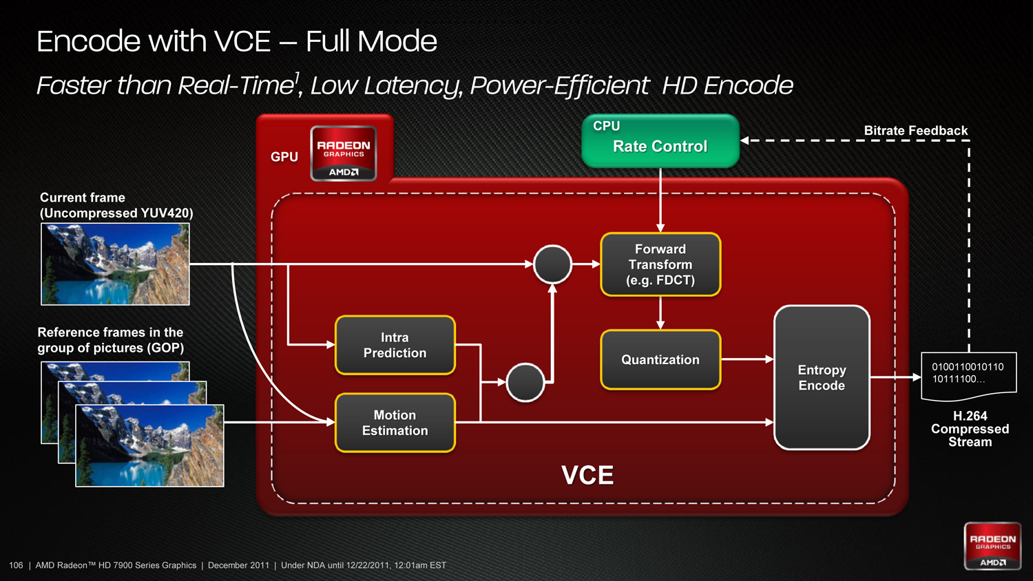
Hybrid Mode is where AMD takes things a step further, by throwing the compute resources of the GPU back into the mix. In Hybrid Mode only Entropy Encode is handled by fixed function hardware (this being a highly serial process that was ill suited to a GPU) with all the other steps being handled by the flexible hardware of the GPU. The end goal of Hybrid Mode is that as these other steps are well suited to being done on a GPU, Hybrid Mode will be much faster than even the highly optimized fixed function hardware of Full Mode. Full Mode is already faster than real time – Hybrid Mode should be faster yet.
With VCE AMD is also targeting Quick Sync’s weaknesses regardless of the mode used. Quick Sync has limited tuning capabilities which impacts the quality of the resulting encode. AMD is going to offer more tuning capabilities to allow for a wider range of compression quality. We don’t expect that it will be up to the quality standards of X264 and other pure-software encoders that can generate archival quality encodes, but if AMD is right it should be closer to archival quality than Quick Sync was.
The catch right now is that VCE is so new that we can’t test it. The hardware is there and we’re told it works, but the software support for it is lacking as none of AMD’s partners have added support for it yet. On the positive side this means we’ll be able to test it in-depth once the software is ready as opposed to quickly testing it in time for this review, however the downside is that we cannot comment on the speed or quality at this time. Though with the 7970 not launching until next year, there’s time for software support to be worked out before the first Southern Islands card ever goes on sale.
Moving on, while encoding has been significantly overhauled decoding will remain largely the same. AMD doesn’t refer to the Universal Video Decoder on Tahiti as UVD3, but the specifications match UVD3 as we’ve seen on Cayman so we believe it to be the same decoder. The quality may have been slightly improved as AMD is telling us they’ve scored 200 on HQV 2.0 – the last time we scored them they were at 197 – but HQV is a partially subjective benchmark.
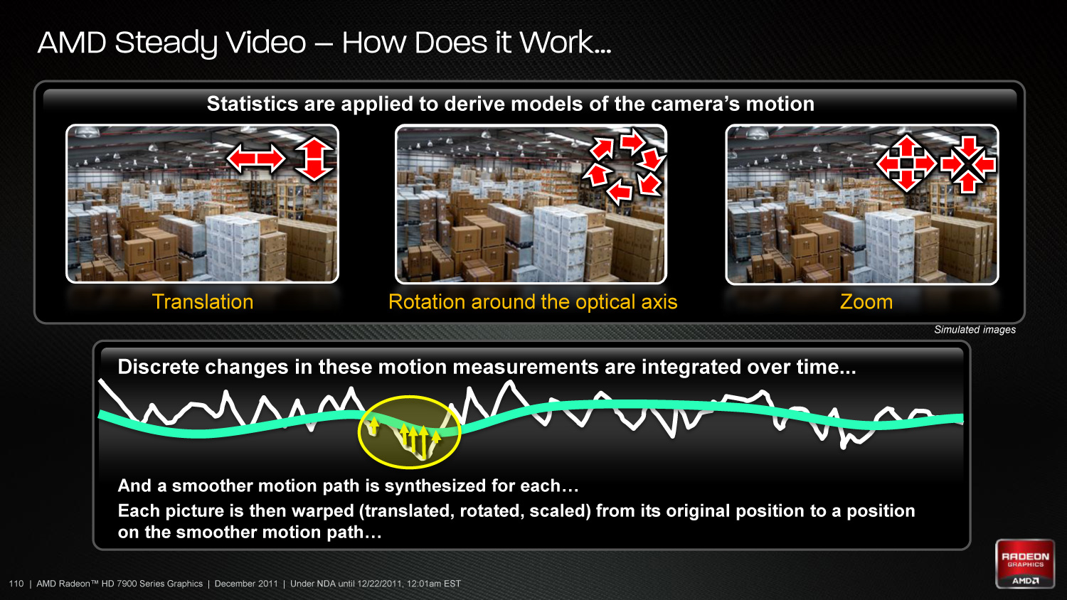
Finally, with Southern Islands AMD is introducing Steady Video 2.0, thesuccessor to Steady Video that was introduced with the Llano APU last year. Steady Video 2.0 adds support for interlaced and letter/pillar boxed content, along with a general increase in the effectiveness of the steadying effect. What makes this particularly interesting is that Steady Video implements a new GCN architecture instruction, Quad Sum of Absolute Differences (QSAD), which combines regular SAD operations with alignment operations into a single instruction. As a result AMD can now execute SADs at a much higher rate so long as they can be organized into QSADs, which is one of the principle reasons that AMD was able to improve Steady Video as it’s a SAD-heavy operation. QSAD extends to more than just Steady Video (AMD noted that it’s also good for other image analysis operations), but Steady Video is going to be the premiere use for it.
PCI Express 3.0: More Bandwidth For Compute
It may seem like it’s still fairly new, but PCI Express 2 is actually a relatively old addition to motherboards and video cards. AMD first added support for it with the Radeon HD 3870 back in 2008 so it’s been nearly 4 years since video cards made the jump. At the same time PCI Express 3.0 has been in the works for some time now and although it hasn’t been 4 years it feels like it has been much longer. PCIe 3.0 motherboards only finally became available last month with the launch of the Sandy Bridge-E platform and now the first PCIe 3.0 video cards are becoming available with Tahiti.
But at first glance it may not seem like PCIe 3.0 is all that important. Additional PCIe bandwidth has proven to be generally unnecessary when it comes to gaming, as single-GPU cards typically only benefit by a couple percent (if at all) when moving from PCIe 2.1 x8 to x16. There will of course come a time where games need more PCIe bandwidth, but right now PCIe 2.1 x16 (8GB/sec) handles the task with room to spare.
So why is PCIe 3.0 important then? It’s not the games, it’s the computing. GPUs have a great deal of internal memory bandwidth (264GB/sec; more with cache) but shuffling data between the GPU and the CPU is a high latency, heavily bottlenecked process that tops out at 8GB/sec under PCIe 2.1. And since GPUs are still specialized devices that excel at parallel code execution, a lot of workloads exist that will need to constantly move data between the GPU and the CPU to maximize parallel and serial code execution. As it stands today GPUs are really only best suited for workloads that involve sending work to the GPU and keeping it there; heterogeneous computing is a luxury there isn’t bandwidth for.

The long term solution of course is to bring the CPU and the GPU together, which is what Fusion does. CPU/GPU bandwidth just in Llano is over 20GB/sec, and latency is greatly reduced due to the CPU and GPU being on the same die. But this doesn’t preclude the fact that AMD also wants to bring some of these same benefits to discrete GPUs, which is where PCI e 3.0 comes in.
With PCIe 3.0 transport bandwidth is again being doubled, from 500MB/sec per lane bidirectional to 1GB/sec per lane bidirectional, which for an x16 device means doubling the available bandwidth from 8GB/sec to 16GB/sec. This is accomplished by increasing the frequency of the underlying bus itself from 5 GT/sec to 8 GT/sec, while decreasing overhead from 20% (8b/10b encoding) to 1% through the use of a highly efficient 128b/130b encoding scheme. Meanwhile latency doesn’t change – it’s largely a product of physics and physical distances – but merely doubling the bandwidth can greatly improve performance for bandwidth-hungry compute applications.
As with any other specialized change like this the benefit is going to heavily depend on the application being used, however AMD is confident that there are applications that will completely saturate PCIe 3.0 (and thensome), and it’s easy to imagine why.
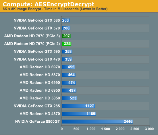
Even among our limited selection compute benchmarks we found something that directly benefitted from PCIe 3.0. AESEncryptDecrypt, a sample application from AMD’s APP SDK, demonstrates AES encryption performance by running it on square image files. Throwing it a large 8K x 8K image not only creates a lot of work for the GPU, but a lot of PCIe traffic too. In our case simply enabling PCIe 3.0 improved performance by 9%, from 324ms down to 297ms.
Ultimately having more bandwidth is not only going to improve compute performance for AMD, but will give the company a critical edge over NVIDIA for the time being. Kepler will no doubt ship with PCIe 3.0, but that’s months down the line. In the meantime users and organizations with high bandwidth compute workloads have Tahiti.
Managing Idle Power: Introducing ZeroCore Power
AMD has been on an idle power crusade for years now. Their willingness to be early adopters of new memory standards has allowed them to offer competitive products on narrower (and thereby cheaper) memory buses, but the tradeoff is that they get to experience the problems that come with the first revision of any new technology.
The most notable case where this has occurred would be the Radeon HD 4870 and 4890, the first cards to use GDDR5. The memory performance was fantastic; the idle power consumption was not. At the time AMD could not significantly downclock their GDDR5 products, resulting in idle power usage that approached 50W. Since then Cypress introduced a proper idle mode, allowing AMD to cut their idle power usage to 27W, while AMD has continued to further refine their idle power consumption.
With the arrival of Southern Islands comes AMD’s latest iteration of their idle power saving technologies. For 7970 AMD has gotten regular idle power usage down to 15W, roughly 5W lower than it was on the 6900 series. This is accomplished through a few extra tricks such as framebuffer compression, which reduce the amount of traffic that needs to move over the relatively power hungry GDDR5 memory bus.
However the big story with Southern Islands for idle power consumption isn’t regular idle, rather it’s “long idle.” Long idle is AMD’s term for any scenarios where the GPU can go completely idle, that is where it doesn’t need to do any work at all. For desktop computers this would primarily be for when the display is put to sleep, as the GPU does not need to do at work when the display itself can’t show anything.
Currently video cards based on AMD’s GPUs can cut their long idle power consumption by a couple of watts by turning off any display transmitters and their clock sources, but the rest of the GPU needs to be minimally powered up. This is what AMD seeks to change.
With Southern Islands AMD is introducing ZeroCore Power, their long idle power saving technology. By implementing power islands on their GPUs AMD can now outright shut off most of the functional units of a GPU when the GPU is going unused, leaving only the PCIe bus interface and a couple other components active. By doing this AMD is able to reduce their power consumption from 15W at idle to under 3W in long idle, a power level low enough that in a desktop the power consumption of the video card becomes trivial. So trivial in fact that with under 3W of heat generation AMD doesn’t even need to run the fan – ZeroCore Power shuts off the fan as it’s rendered an unnecessary device that’s consuming power.
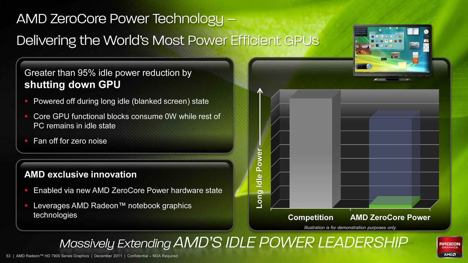
Ultimately ZeroCore Power isn’t a brand new concept, but this is the first time we’ve seen something quite like this on the desktop. Even AMD will tell you the idea is borrowed from their mobile graphics technology, where they need to be able to power down the GPU completely for power savings when using graphics switching capabilities. But unlike mobile graphics switching AMD isn’t fully cutting off the GPU, rather they’re using power islands to leave the GPU turned on in a minimal power state. As a result the implementation details are very different even if the outcomes are similar. At the same time a technology like this isn’t solely developed for desktops so it remains to be seen how AMD can leverage it to further reduce power consumption on the eventual mobile Southern Islands GPUs.
Of course as impressive as sub-3W long idle power consumption is on a device with 4.3B transistors, at the end of the day ZeroCore Power is only as cool as the ways it can be used. For gaming cards such as the 7970 AMD will be leveraging it not only as a way to reduce power consumption when driving a blanked display, but more importantly will be leveraging it to improve the power consumption of CrossFire. Currently AMD’s Ultra Low Power State (ULPS) can reduce the idle power usage of slave cards to a lower state than the master card, but the GPUs must still remain powered up. Just as with long idle, ZeroCore Power will change this.
Fundamentally there isn’t a significant difference between driving a blank display and being a slave card card in CrossFire, in both situations the video card is doing nothing. So AMD will be taking ZeroCore Power to its logical conclusion by coupling it with CrossFire; ZeroCore Power will put CrossFire slave cards in ZCP power state whenever they’re not in use. This not only means reducing the power consumption of the slave cards, but just as with long idle turning off the fan too. As AMD correctly notes, this virtually eliminates the idle power penalty for CrossFire and completely eliminates the idle noise penalty. With ZCP CrossFire is now no noisier and only ever so slightly more power hungry than a single card at idle.
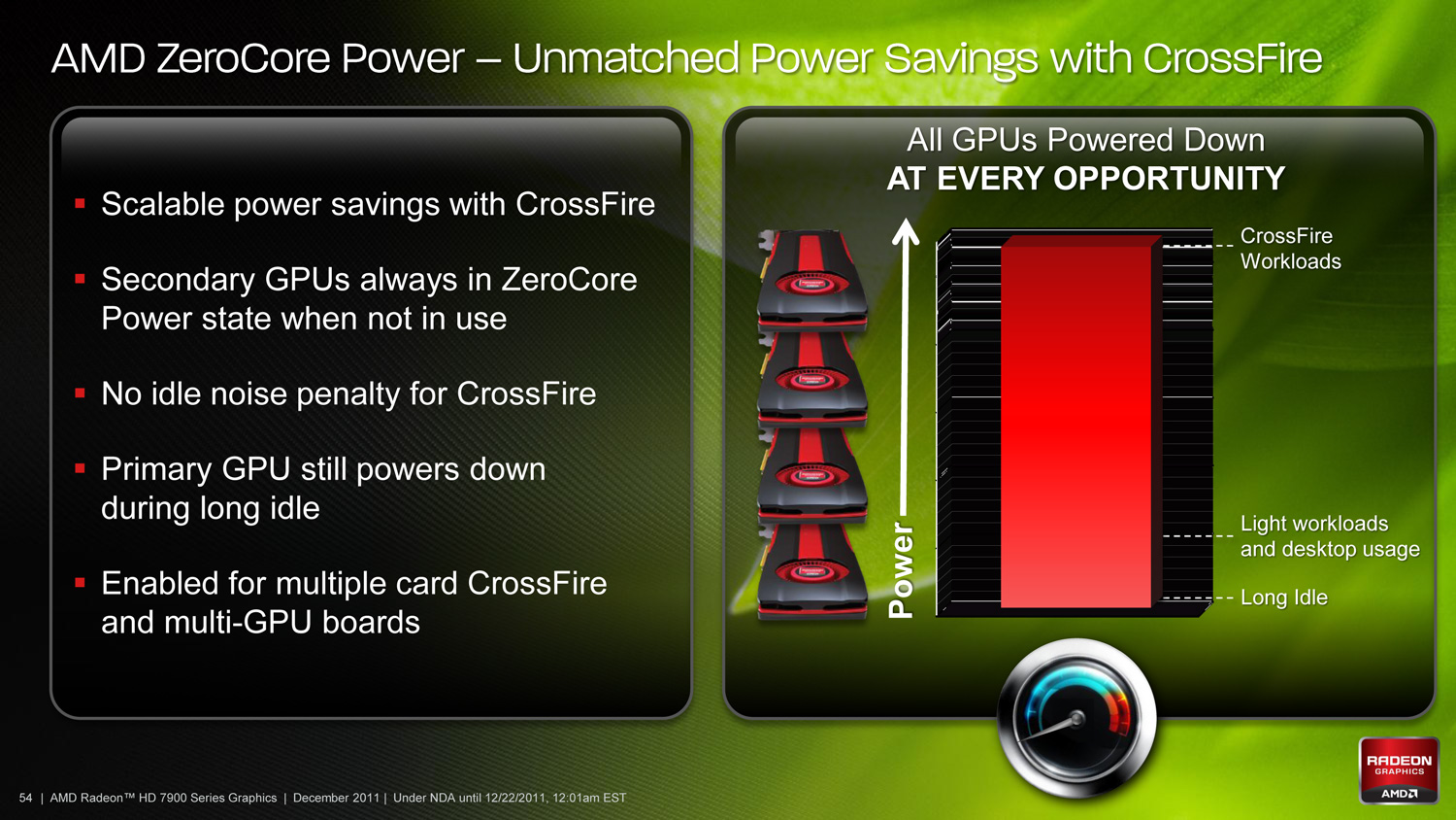
Furthermore the benefits of ZCP in CrossFire not only apply to multiple cards, but multiple-GPU cards too. When AMD launches their eventual multi-GPU Tahiti card the slave GPU can be put in a ZCP state, leaving only the master GPU and the PCIe bridge active. Coupled with ZCP on the master GPU when in long idle and even a beastly multi-GPU card should be able to reduce its long idle power consumption to under 10W after accounting for the PCIe bridge.
Meanwhile as for load power consumption, not a great deal has changed from Cayman. AMD’s PowerTune throttling technology will be coming to the entire Southern Islands lineup, and it will be implemented just as it was in Cayman. This means it remains operationally the same by calculating the power draw of the card based on load, and then altering clockspeeds in order to keep the card below its PowerTune limit. For the 7970 the limit is the same as it was for the 6970: 250W, with the ability to raise or lower it by 20% in the Catalyst Control Center.
On that note, at this time the only way to read the core clockspeed of the 7970 is through AMD’s drivers, which don’t reflect the current status of PowerTune. As a result we cannot currently tell when PowerTune has started throttling. If you recall our 6970 results we did find a single game that managed to hit PowerTune’s limit: Metro 2033. So we have a great deal of interest in seeing if this holds true for the 7970 or not. Looking at frame rates this may be the case, as we picked up 1.5fps on Metro after raising the PowerTune limit by 20%. But at 2.7% this is on the edge of being typical benchmark variability so we’d need to be able to see the core clockspeed to confirm it.
Image Quality: Anisotropic Filtering Tweaks & Tessellation Speed
Since the launch of Evergreen AMD has continued to tweak their anisotropic filtering quality. Evergreen introduced angle-independent filtering, and with the 6000 series AMD tweaked their AF algorithm to better handle high frequency textures. With Southern Islands that trend continues with another series of tweaks.
For Southern Islands AMD has changed the kernel weights of their anisotropic filtering mechanism in order to further reduce shimmering of high frequency textures. The algorithm itself remains unchanged and as does performance, but image quality is otherwise improved. Admittedly these AF changes seem to be targeting increasingly esoteric scenarios – we haven’t seen any real game where the shimmering matches the tunnel test – but we’ll gladly take any IQ improvements we can get.
Since AMD’s latest changes are focused on reducing shimmering in motion we’ve put together a short video of the 3D Center Filter Tester running the tunnel test with the 7970, the 6970, and GTX 580. The tunnel test makes the differences between the 7970 and 6970 readily apparent, and at this point both the 7970 and GTX 580 have similarly low levels of shimmering.
While we’re on the subject of image quality, had you asked me two weeks ago what I was expecting with Southern Islands I would have put good money on new anti-aliasing modes. AMD and NVIDIA have traditionally kept parity with AA modes, with both implementing DX9 SSAA with the previous generation of GPUs, and AMD catching up to NVIDIA by implementing Enhanced Quality AA (their version of NVIDIA’s CSAA) with Cayman. Between Fermi and Cayman the only stark differences are that AMD offers their global faux-AA MLAA filter, while NVIDIA has support for true transparency and super sample anti-aliasing on DX10+ games.
Thus I had expected AMD to close the gap from their end with Southern Islands by implementing DX10+ versions of Adaptive AA and SSAA, but this has not come to pass. AMD has not implemented any new AA modes compared to Cayman, and as a result AAA and SSAA continue to only available in DX9 titles. And admittedly alpha-to-coverage support does diminish the need for these modes somewhat, but one only needs to fire up our favorite testing game, Crysis, to see the advantages these modes can bring even to DX10+ games. What’s more surprising is that it was AMD that brought AA IQ back to the forefront in the first place by officially adding SSAA, so to see them not continue that trend is surprising.
As a result for the time being there will continue to be an interesting division in image quality between AMD and NVIDIA. AMD still maintains an advantage with anisotropic filtering thanks to their angle-independent algorithm, but NVIDIA will have better anti-aliasing options in DX10+ games (ed: and Minecraft). It’s an unusual status quo that apparently will be maintained for quite some time to come.
Update: AMD has sent us a response in regard to our question about DX10+ SSAA
Basically the fact that most new game engines are moving to deferred rendering schemes (which are not directly compatible with hardware MSAA) has meant that a lot of attention is now being focused on shader-based AA techniques, like MLAA, FXAA, and many others. These techniques still tend to lag MSAA in terms of quality, but they can run very fast on modern hardware, and are improving continuously through rapid iteration. We are continuing work in this area ourselves, and we should have some exciting developments to talk about in the near future. But for now I would just say that there is a lot more we can still do to improve AA quality and performance using the hardware we already have.
Regarding AAA & SSAA, forcing these modes on in a general way for DX10+ games is problematic from a compatibility standpoint due to new API features that were not present in DX9. The preferred solution would be to have games implement these features natively, and we are currently investigating some new ways to encourage this going forward.
Finally, while AMD may be taking a break when it comes to anti-aliasing they’re still hard at work on tessellation. As we noted when discussing the Tahiti/GCN architecture AMD’s primitive pipeline is still part of their traditional fixed function pipeline, and just as with Cayman they have two geometry engines that can process up to two triangles per clock. On paper at least Tahiti doesn’t significantly improve AMD’s geometry performance, but as it turns out there’s a great deal you can do to improve geometry performance without throwing more geometry hardware at the task.
For Southern Islands AMD has implemented several techniques to boost the efficiency of their geometry engines. A larger parameter cache is a big part of this, but AMD has also increased vertex re-use and off-chip buffering. As such while theoretical geometry throughput is unchanged outside of the clockspeed differences between 7970 and 6970, AMD will be making better use of the capabilities of their existing geometry pipeline.
By AMD’s numbers these enhancements combined with the higher clockspeed of the 7970 versus the 6970 give it anywhere between a 1.7x and 4x improvement in tessellation performance. In our own tests the improvements aren’t quite as great, but they’re still impressive. Going by the DX11DetailTessellation sample program the 7970 has better performance than the GTX 580 at both normal and high tessellation factors (and particularly at high tessellation factors), while under Unigine Heaven – a tessellation-heavy synthetic benchmark – the 7970 leads the GTX 580 by over 20%. Or compared to the 6970 the difference is even more stark, with the 7970 leading the 6970 by about 55% in both of these benchmarks.
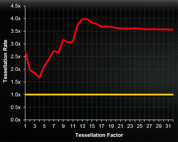
Of course both of these benchmarks are synthetic and real world performance can (and will) differ, but it does prove that AMD’s improvements in tessellation efficiency really do matter. Even though the GTX 580 can push up to 8 triangles/clock, it looks like AMD can achieve similar-to-better tessellation performance in many situations with their Southern Islands geometry pipeline at only 2 triangles/clock.
Though with that said, we’re still waiting to see the “killer app” for tessellation in order to see just how much tessellation is actually necessary. Current games (even BF3) are DX10 games with tessellation added as an extra instead of being a fundamental part of the rendering pipeline. There are a wide range of games from BF3 to HAWX 2 using tessellation to greatly different degrees and none of them really answer the question of how much tessellation is actually necessary. Both AMD and NVIDIA have made tessellation performance a big part of their marketing pushes, so there’s a serious question over whether games will be able to utilize that much geometry performance, or if AMD and NVIDIA are in another synthetic numbers war.
Drivers & ISV Relations
As we noted last week with the release of the Catalyst 12.1 preview, AMD has a lot of technical and reputational debt to dig themselves out of when it comes to their Catalyst drivers. AMD dropped the ball this fall a number of times, failing to deliver on appropriate drivers for Rage, Battlefield 3, and The Elder Scrolls V: Skyrim in a timely manner. This isn’t something AMD is shying away from either – they know they screwed up and they’ll admit as much – but the question remains of how they intend to improve from there. Now that they once again have the leading single-GPU video card they need to have the leading drivers to run it.
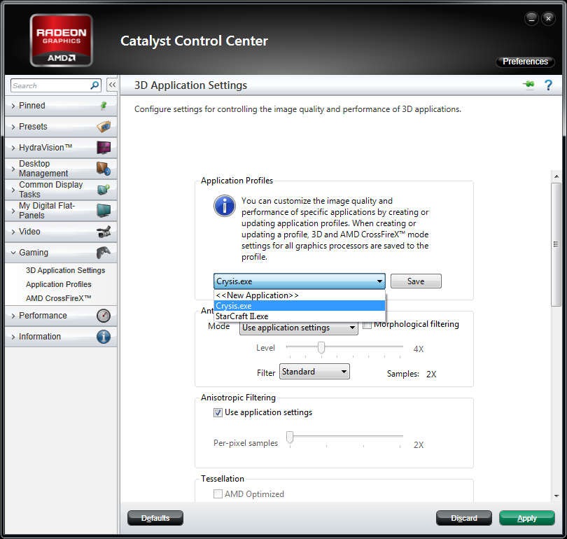
Part of this redemption will come from the addition of new features, if only to reach parity with NVIDIA. Catalyst 12.1 introduced custom application profiles, while as we discussed with Eyefinity, Catalyst 12.2 will add to AMD’s suite of Eyefinity features with custom resolutions and the ability to relocate the Windows task bar. Furthermore AMD has features in the development pipeline for their Catalyst drivers for introduction later this year, but at this point it’s too early to talk about them.
But new features alone can’t fix every single thing that has ailed AMD in the past year, so the question remains: how does AMD intend to fix their poor delivery of optimized drivers for new games? It’s a question AMD cannot (or will not) completely answer in detail, but it’s a question for which there’s at least part of an answer.
The fundamental answer is more. More developers, more quality assurance, and above all more money. By all accounts NVIDIA sinks a lot of money into driver development and ISV and it usually shows. AMD is going to spend more resources on driver development at home and this is going to help a great deal, but at the same time it would seem that they’ve finally come to realize that great ISV relationships require that AMD be more proactive than how they’ve been in the past.
ISV relations covers a large umbrella of activities. Not only does this mean providing support to developers who request it, but it means providing cross-promotion marketing, encouraging developers to make use of your features (if only to help spur the creation of the killer app), and actively seeking out important development houses so that AMD’s interests and concerns are represented and represented early. It’s been said that the most important thing NVIDIA ever did with ISV relations was to send out their own engineers to development houses on their own dime to provide free support – essentially investing at least a small amount of money into a major game. The payoff of this was that NVIDIA was literally there to represent their interests, and conversely they had a chance to evaluate the game early and get to work on optimizations and SLI support well before it shipped. Snark about TWIMTBP aside, that’s where NVIDIA has raised the bar with ISV relations. That’s what AMD needs to follow.
To that extent AMD has reorganized the budget process for their ISV relations department. Neal Robison, the director of ISV relations, now directly controls a much larger ISV relations budget, whereas previously the ISV relations budget was apparently controlled by several parties. Having more funding for ISV relations won’t solve AMD’s issues on its own – It’s all about how that money is spent – but clearly AMD is on the right path by being able to afford to be more proactive about their ISV relationships.
Whether these changes will pay off as AMD is expecting them to remains to be seen, but from our discussions it’s apparent that AMD is trying harder than ever before. A great product requires good hardware and good software; AMD has the former in Tahiti, now it’s time to see if they can deliver on the latter.
Closing out the subject of drivers, AMD is also using the Southern Islands launch to outline their plans for Windows 8. AMD is promising that they will deliver drivers for Windows 8 on the same schedule as they have for Windows 7 and Windows Vista – new drivers will be available for the Windows 8 Beta, RC, and RTM releases. Furthermore as Microsoft has continually iterated on the WDDM driver stack since Vista, AMD will continue to be able to offer a single unified driver that covers all of the WDDM OSes (Vista, 7, and 8).
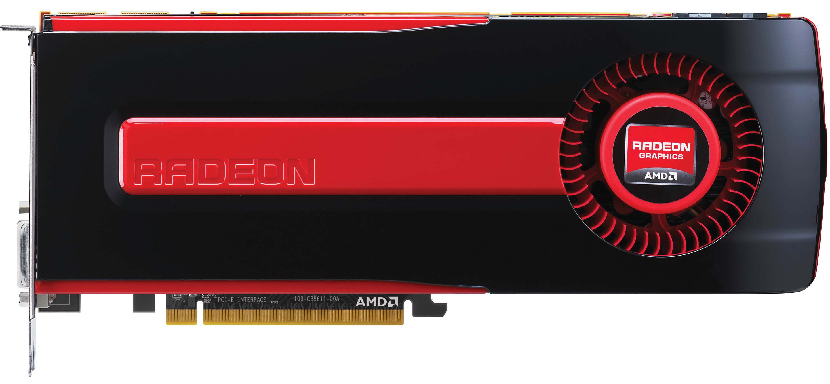
Meet the Radeon HD 7970
Now that we’ve had a chance to discuss the features and the architecture of GCN and Tahiti, we can finally get to the end result: the card. AMD’s first product in the Southern Islands family is the Radeon HD 7970, continuing AMD’s tradition of launching their fastest single-GPU first.
As we’ve already covered in our discussion on GCN/Tahiti’s architecture, Tahiti shares a lot of physical similarities with Cayman, and so then does the 7970 with the 6970. With the 7970 AMD has targeted a very similar power profile as the 6970, and while AMD has not published the typical board power of the 7970 we know the PowerTune limit is 250W, the same as with the 6970. As a result the 7970 is at least superficially designed to work in the same environments/constraints as the 6970.
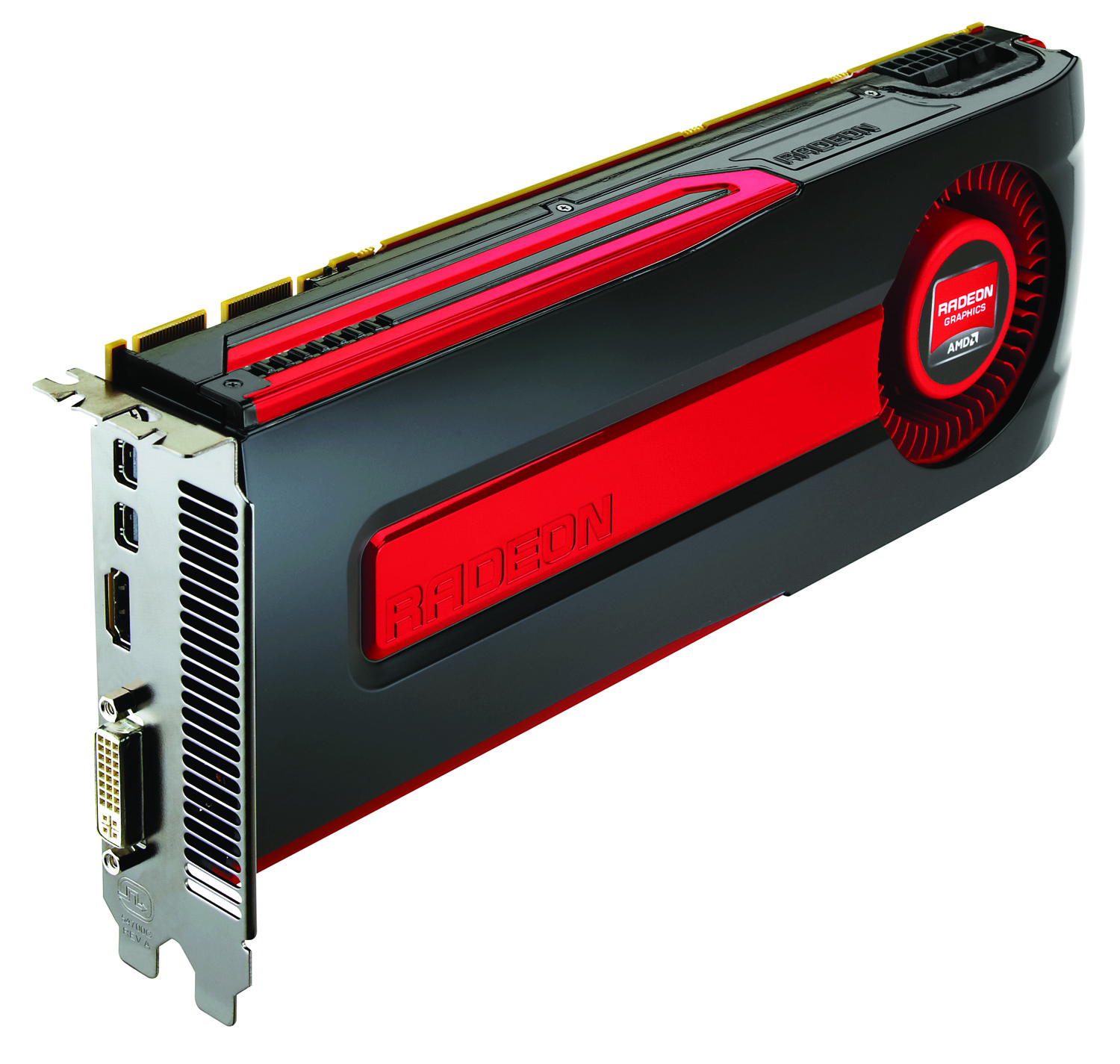
With that said, AMD has not sat idle when it comes to the design of the card – this isn’t just a Tahiti GPU put in a 6970 shell. Livery changes aside it’s clear that the 7970 is a distinct card just from looking at it. AMD’s ill-fated boxy design for their cards is gone; the removable plastic shroud is now once again a rounded design similar to the 5800 series, and this time AMD takes it a step further by slightly rounding off the rear of the card for airflow purposes. Furthermore the shroud is now made of a very hard, very shiny plastic, versus the soft plastic used in past cards.
But the bigger change is on the back of the card, where AMD has completely done away with the backplate. First used in the 5800, backplates help to protect the card from users (and users from the sharp bits of the card), but the tradeoff was that the backplate occupied 2.7mm of space. What’s the significance of 2.7mm? When you’re trying to put these cards adjactent to each other for CrossFire, it’s everything as we have found out.
The boxy design coupled with the backplate meant that the 6900 series used virtually every last millimeter of space they were allowed under the PCIe specification; the cards were so wide that when adjacent it was easy for a card to shift and block the airflow of the neighboring card. The backplate contributed to this problem by consuming 2.7mm of space that could otherwise be used to channel airflow, and as a result it’s gone. AMD’s design doesn’t have the overt wedge that NVIDIA’s does to allow airflow, but it should be enough to keep the cards well enough separated to allow them to breathe when they’re closely together for CrossFire.
Overall the card is 10.5” going by the PCB, but AMD has a metal reinforcement ring/plate running along the entire card that sticks out the rear. After accounting for this plate the total length of the card is just shy of 11”, making the card roughly half an inch longer than the 6970 and 5870. The difference is not huge, but it will make the 7970 ever so slightly harder to fit than the 6970 in space-constrained cases.
Moving on, while AMD has made some changes to the shrouding to improve cooling, they haven’t stopped there. The blower has also been tweaked slightly compared to what we’ve seen on the 6970. The 7970’s blower is a bit larger (~75mm) and the fins are slightly larger to make use of that space. Overall this should improve the amount of air moved at speeds similar to the blower on the 6970, though AMD didn’t provide any numbers.
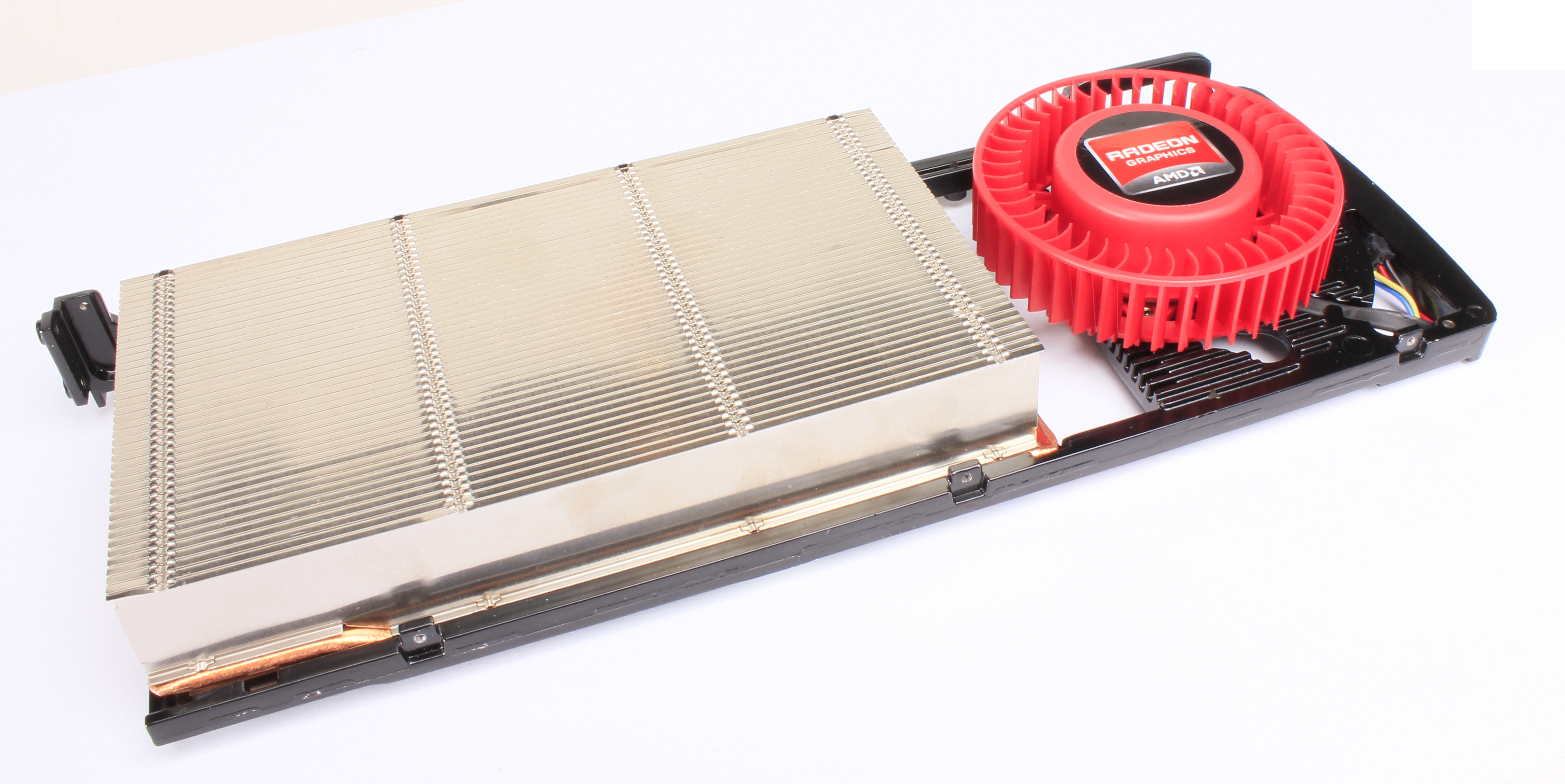
Meanwhile the heatsink is very similar to the 6970’s. As with the 6970 an aluminum heatsink sits on top of a vapor chamber cooler that draws heat from the GPU and other components towards the heatsink. Other than being a bit larger than the 6970 the biggest difference is that AMD is now using the same higher performance phase-change TIM that they used on the 6990, which also means that AMD is highly recommending that the 7970 not be disassembled as the TIM won’t operate nearly as well once it’s been separated. Furthermore as we found out the specific TIM AMD is using is screen printed onto the GPU, so reapplying a new TIM in the same manner is virtually impossible.
Finally, it’s once we move towards the front that we see the biggest change in the name of cooling: AMD has once again moved back to a full slot exhaust vent. As you may recall, starting with the 5800 series AMD moved to a half slot vent configuration so that they could use the other half of the second slot to fit a second DVI port along with their DisplayPort and HDMI ports. The half slot vent did not prove to be a huge problem for the 5800 or 6900 series but it still placed some limits on AMD’s ability to cool their cards and made the process a bit noisier. As the second DVI port has become redundant (more on that later), AMD has opted to get rid of it and go back to using the whole slot for cooling. One way or another though this was probably necessary – looking at our data the 7970 is a bit more power hungry than the 6970 even if the specifications are similar, and as a result AMD needs better cooling to keep parity with the 6970.
Moving on, tweakers will be happy to see that the dual BIOS feature first introduced on the 6900 series is back. The 7970 will feature the same dual BIOS configuration, with a locked factory BIOS (2), and a rewritable BIOS (1) for other uses. As with the 6900 series this is primarily to allow failsafe BIOS flashing, but the implications for GPU unlocking lower tier cards are clear. In fact we’re surprised that AMD included the switch given how rampant 6950 unlocking was, as while it was good PR it must have been bad for their 6970 sales.
Next to the BIOS switch we will find the PCIe power sockets, which given the 250W PowerTune limit of the card mean we’re looking at the same 6+8pin configuration as the 6970. Enthusiasts who caught on to the fact that AMD had to shave some PCIe sockets on the 6900 series should note that the sockets are untouched on the 7970, as the blower now sits above the PCIe sockets. Elsewhere at the front end of the card we’ll find the two CrossFire connectors, and as always when it comes to their high-end cards AMD is supporting up to 3-way CF with the 7970.
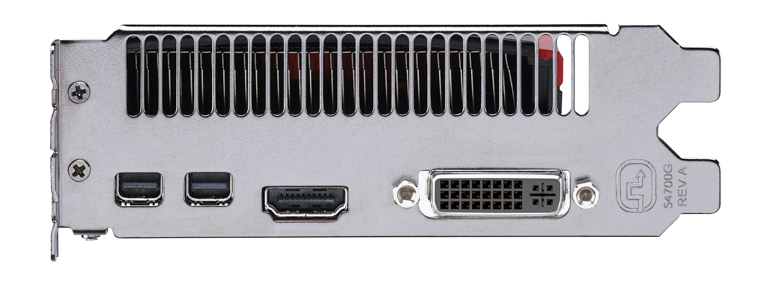
Back to the front of the card we can see AMD’s new Southern Islands port configuration. As you may recall from the 6000 series, with the 6000 series AMD moved from being able to drive 2 dual-link DVI ports (2 sets of paired TMDS transmitters) to being able to drive 1 dual-link DVI port + 1 single-link DVI port, as they removed the 4th TMDS transmitter. Furthermore as AMD has only been able to drive 2 TMDS-type ports at once, the 2nd DVI port was largely redundant as everything it could do the HDMI port could do with a mechanical adaptor.
So for Southern Islands AMD has taken this to its logical conclusion and cut out the 2nd DVI port entirely. There is now a single DL-DVI port, along with an HDMI port and 2 miniDP ports all along a single slot. The 7970 still has the internal logic to drive the same monitor configurations as the 6970, but anyone using the SL-DVI port will now be fed by the HDMI port. In order to make this transition easier on buyers, AMD will be requiring that partners ship both an HDMI to SL-DVI adaptor and an active miniDP to SL-DVI adaptor with their 7970s, so 7970 users will be able to drive up to 3 DVI monitors out of the box, which is actually better than what the 6970 could do. Of course we expect that this will be a limited time offer; once AMD’s partners start putting together cheaper cards later in the 7970’s life, the mDP to SL-DVI adaptor will be the first thing to go.
On that note, for anyone who is curious about idle clockspeeds and power consumption with multiple monitors, it has not changed relative to the 6970. When using a TMDS-type monitor along with any other monitor, AMD has to raise their idle clockspeeds from 350MHz core and 600Mhz memory to 350MHz core and the full 5.5GHz speed for memory, with the power penalty for that being around 30W. Matched timing monitors used exclusively over DisplayPort will continue to be the only way to be able to use multiple monitors without incurring an idle penalty.
Next on the docket we wanted to quickly touch on the subject of RAM. As with their past cards AMD has outfitted the 7970 with RAM rated beyond their memory speed requirements, in this case the 7970 is outfitted with 6GHz modules even though it only needs to operate at 5.5GHz. We haven’t been able to take the card apart so we haven’t seen whose modules AMD is using, but we strongly suspect they’re the same 2Gb Hynix modules the reference 6970 used.
With the move to a 384bit bus AMD has increased the chip count from 8 to 12, and the total RAM size from 2GB to 3GB. As games are only now starting to effectively use more than 1GB of RAM this should offer plenty of headroom for future games, above and beyond even their existing 2GB cards.
At the same time with the move to a 384bit bus this has raised the question of where AMD goes from here. It’s well published that GDDR5 is an intricate memory technology to work with, with the memory bus being the hardest part. To run a 384bit bus at 5.5GHz is quite the accomplishment (NVIDIA didn’t get nearly that high with Fermi), but it also means that we’re near the end of the road for GDDR5. While GDDR5 is rated for up to 7GHz in the real world buses will never be able to scale quite that well and the required memory voltages are on the high side. Meanwhile a 512bit GDDR5 bus is possible but would be even more expensive and difficult than a 384bit bus, and it’s safe to say that’s not the preferred route.
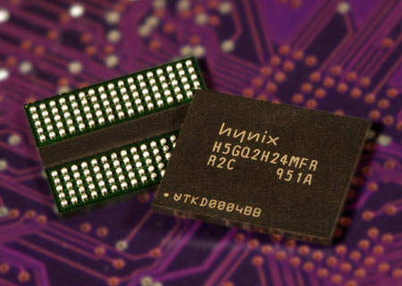
So what comes after GDDR5? At this point AMD tells us that they’re looking at a few different things, but of course it’s far too early to discuss anything in detail. The JEDEC has not passed anything such as a GDDR6 standard, though we expect whatever technology AMD will eventually use will come out of the JEDEC. But if nothing else at this point it’s safe to assume that by the time we’re on 20nm GPUs we won’t be using GDDR5.
Finally, while we haven’t had a chance to tinker with overclocking due to our limited time with the 7970, but AMD is telling us that the 7970 is going to be good overclocker. Most cards should be able to hit 1GHz or higher on the core clock and 6GHz or higher on the memory clock with little effort even with the reference cooler, but the tradeoff will of course be in power consumption and noise, as you’ll need to increase the PowerTune limits to make those overclocks matter.
The Test
Starting with the launch of the 7970 we will be using our new GPU testbed, replacing both our hardware and most of our benchmarks. On the hardware side we’re using an Intel Core i7 3960X overclocked to 4.3GHz on an EVGA X79 SLI motherboard, giving us access to PCIe 3.0 while keeping most CPU bottlenecks at bay. While we’re only looking at a single card today, based on some informal surveys for multi-GPU testing we will continue to test our cards adjacent to each other to represent the worst case scenario, as it turns out there are a number of users out there who do use that arrangement even if they’re not in the majority.
On the software side we’ve refreshed most of our benchmarks; the suite is tilted towards DX11, but there are still enough DX9/10 tests to get a good idea of how new cards compare to pre-DX11 cards. On that note I know we have a lot of Skyrim fans out there, and while we wanted to include Skyrim benchmark we’re having trouble coming up with any good test cases (that don’t involve INI hacking) that aren’t incredibly CPU limited. If you have any suggestions, please drop me a line.
For drivers on AMD’s cards we’re using AMD’s beta 8.921.2-111215a drivers, which identify themselves as Catalyst 11.12 but are otherwise indistinguishable from the Catalyst 12.1 preview released last week. On that note, for those of you who have been asking about support for D3D11 Driver Command Lists – an optional D3D11 feature that helps with multithreaded rendering and is NVIDIA’s secret sauce for Civilization V – AMD has still not implemented support for it as of this driver.

For NVIDIA’s cards we’re using NVIDIA’s latest beta driver, 290.36.
Finally, as we’ve only had a limited amount of time with the 7970, we’ve narrowed our suite of cards just slightly in order to make the deadline. For those of you curious about how middle-tier cards such as the GTX 560 series and the Radeon HD 6800 series or various multi-card SLI and CrossFire setups compare, we’ll be adding new results to Bench throughout the rest of the month, and Eyefinity soon after that. For the time being since we only have a single card, we’re focusing on single card results with a single monitor.
| CPU: | Intel Core i7-3960X @ 4.3GHz |
| Motherboard: | EVGA X79 SLI |
| Chipset Drivers: | Intel 9.2.3.1022 |
| Power Supply: | Antec True Power Quattro 1200 |
| Hard Disk: | Samsung 470 (240GB) |
| Memory: | G.Skill Ripjaws DDR3-1867 4 x 4GB (8-10-9-26) |
| Video Cards: |
AMD Radeon HD 7970 AMD Radeon HD 6990 AMD Radeon HD 6970 AMD Radeon HD 6950 AMD Radeon HD 5870 AMD Radeon HD 5850 AMD Radeon HD 4870 AMD Radeon HD 3870 NVIDIA GeForce GTX 590 NVIDIA GeForce GTX 580 NVIDIA GeForce GTX 570 NVIDIA GeForce GTX 470 NVIDIA GeForce GTX 285 NVIDIA GeForce 8800GT |
| Video Drivers: |
NVIDIA ForceWare 290.36 Beta AMD Catalyst Beta 8.921.2-111215a |
| OS: | Windows 7 Ultimate 64-bit |
Crysis: Warhead
Kicking things off as always is Crysis: Warhead. It’s no longer the toughest game in our benchmark suite, but it’s still a technically complex game that has proven to be a very consistent benchmark. Thus even 4 years since the release of the original Crysis, “but can it run Crysis?” is still an important question, and the answer continues to be “no.” While we’re closer than ever, full Enthusiast settings at a 60fps is still beyond the grasp of a single-GPU card.
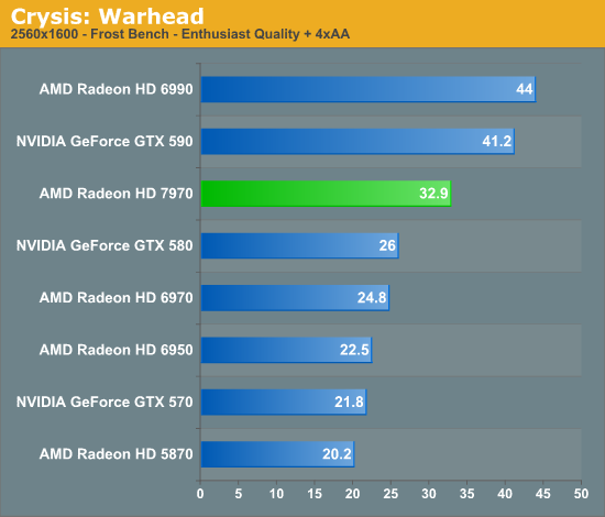
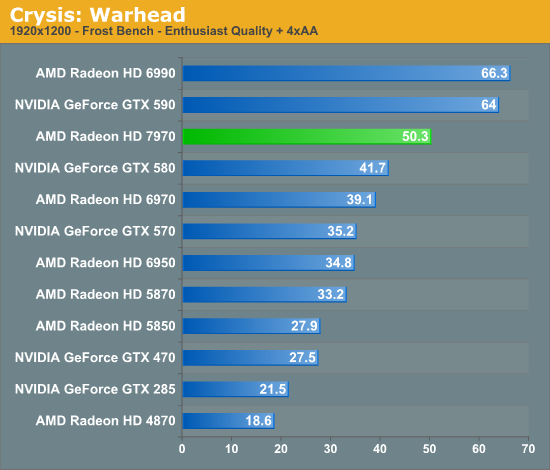
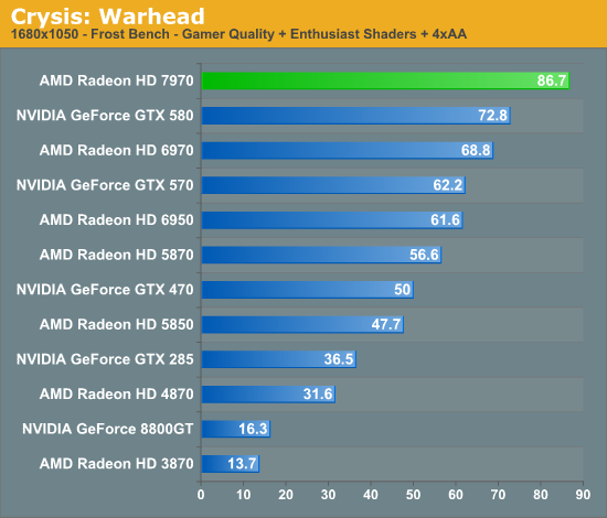
This year we’ve finally cranked our settings up to full Enthusiast quality for 2560 and 1920, so we can finally see where the bar lies. To that extent the 7970 is closer than any single-GPU card before as we’d imagine, but it’s going to take one more jump (~20%) to finally break 60fps at 1920.
Looking at the 7970 relative to other cards, there are a few specific points to look at; the GTX 580 is of course its closest competitor, but we can also see how it does compared to AMD’s previous leader, the 6970, and how far we’ve come compared to DX10 generation cards.
One thing that’s clear from the start is that the tendency for leads to scale with the resolution tested still stands. At 2560 the 7970 enjoys a 26% lead over the GTX 580, but at 1920 that’s only a 20% lead and it shrinks just a bit more to 19% at 1680. Even compared to the 6970 that trend holds, as a 32% lead is reduced to 28% and then 26%. If the 7970 needs high resolutions to really stretch its legs that will be good news for Eyefinity users, but given that most gamers are still on a single monitor it may leave AMD closer to 40nm products in performance than they’d like.
Speaking of 40nm products, both of our dual-GPU entries, the Radeon HD 6990 and GeForce GTX 590 are enjoying lofty leads over the 7970 even with the advantage of its smaller fabrication process. To catch up to those dual-GPU cards from the 6970 would require a 70%+ increase in performance, and even with a full node difference it’s clear that this is not going to happen. Not that it’s completely out of reach for the 7970 once you start looking at overclocking, but the reduction in power usage when moving from TSMC 40nm to 28nm isn’t nearly large enough to make that happen while maintaining the 6970’s power envelope. Dual-GPU owners will continue to enjoy a comfortable lead over even the 7970 for the time being, but with the 7970 being built on a 28nm process the power/temp tradeoff for those cards is even greater compared to 40nm products.
Meanwhile it’s interesting to note just how much progress we’ve made since the DX10 generation though; at 1920 the 7970 is 130% faster than the GTX 285 and 170% faster than the Radeon HD 4870. Existing users who skip a generation are a huge market for AMD and NVIDIA, and with this kind of performance they’re in a good position to finally convince those users to make the jump to DX11.
Finally it should be noted that Crysis is often a good benchmark for predicting overall performance trends, and as you will see it hasn’t let us down here. How well the 7970 performs relative to its competition will depend on the specific game, but 20-25% isn’t too far off from reality.
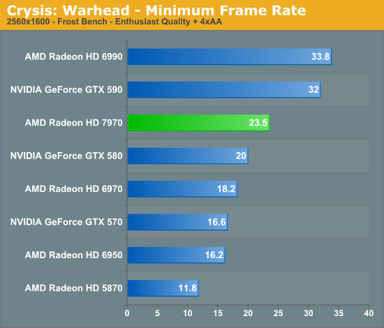
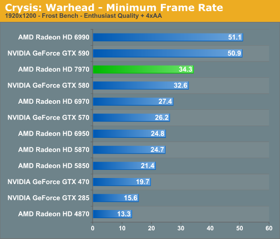
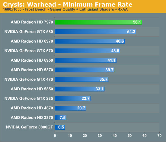
Looking at our minimum framerates it’s a bit surprising to see that while the 7970 has a clear lead when it comes to average framerates the minimums are only significantly better at 2560. At that resolution the lowest framerate for the 7970 is 23.5 versus 20 for the GTX 580, but at 1920 that becomes a 2fps, 5% difference. It’s not that the 7970 was any less smooth in playing Crysis, but in those few critical moments it looks to be dipping a bit more than the GTX 580.
Compared to the 6970 on the other hand the minimum framerate difference is much larger and much more consistent. At 2560 the 7970’s minimums are 29% better, and even at lower resolutions it holds at around 25%. Clearly even with AMD’s new architecture their designs still inherit some of the traits of their old designs.
Metro: 2033
Paired with Crysis as our second behemoth FPS is Metro: 2033. Metro gives up Crysis’ lush tropics and frozen wastelands for an underground experience, but even underground it can be quite brutal on GPUs, which is why it’s also our new benchmark of choice for looking at power/temperature/noise during a game. If its sequel due this year is anywhere near as GPU intensive then a single GPU may not be enough to run the game with every quality feature turned up.
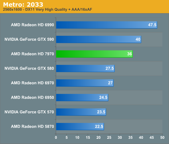
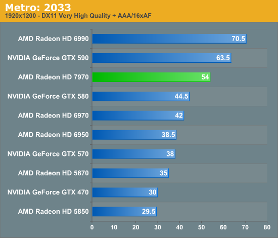
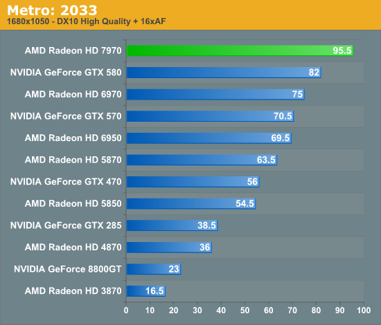
As often as we concern ourselves with Crysis and 60fps, with Metro it’s a struggle just to break 30fps. The 7970 becomes the first video card that can accomplish this at 2560 though it’s going to need quite a bit more performance to run Metro fluidly from start to end.
Compared to the GTX 580 the 7970’s lead in Metro is similar, but the scaling with resolution is even more pronounced. At 2560 it’s ahead by 30%, while at 1920 this drops to 21%, and finally at 1680 it’s only 16%. Meanwhile compared to the 6970 the response is much flatter; 33% at 2560, 28% at 1920, and 27% at 1680. From this data it’s becoming increasingly evident that the value proposition of the 7970 is going to hinge on not only what you consider its competitors to be, but what resolutions you would use it at.
While we’re on the subject of Metro, this is a good time to bring up the performance of the 5870, the forerunner of the DX11 generation. The performance of the 7970 may only be 20-30% higher than its immediate predecessors, but that’s not to say that performance hasn’t increased a great deal more over the full 2 year period of the 40nm cycle. The 7970 leads the 5870 by 50-60% here and in a number of other games, and while this isn’t as great as some past leaps it’s clear that there’s still plenty of growth in GPU performance occurring.
DiRT 3
For racing games our racer of choice continues to be DiRT, which is now in its 3rd iteration. Codemasters uses the same EGO engine between its DiRT, F1, and GRID series, so the performance of EGO is has been relevant for a number of number of racing games over the years.
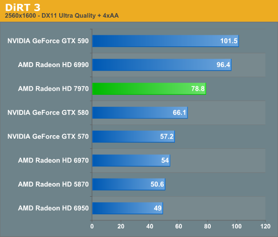
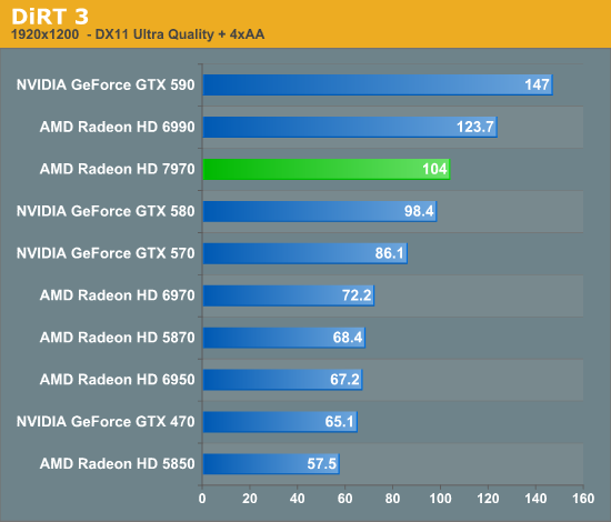
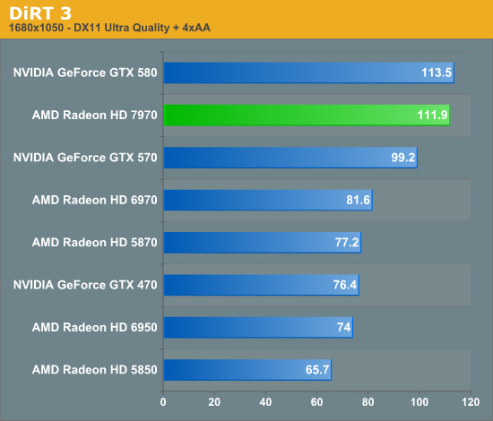
With DiRT 2 NVIDIA often held a slight edge in performance, and due to the reuse of the EGO engine this hasn’t really changed in DiRT 3. As a result the 7970 is still faster than the GTX 580, but not by as much as in other games. At 2560 this manifests itself as a 19% lead, while at 1920 it’s down to 6%, and embarrassingly enough at 1680 the 7970 actually falls behind the GTX 580 by just a hair. DiRT 3 is not particularly shader heavy so that may be part of the reason that the 7970 can’t easily clear the GTX 580 here, but that doesn’t fully explain what we’re seeing. At the end of the day this is all academic since everything north of the GTX 570 can clear 60fps even at 2560, but it would be nice to eventually figure out why NVIDIA does better than average here.
Meanwhile compared to the 6970 the 7970 enjoys one of its bigger leads. Here the 7970 leads by about 45% at 2560 and 1920, and finally falls slightly to 37% at 1680.
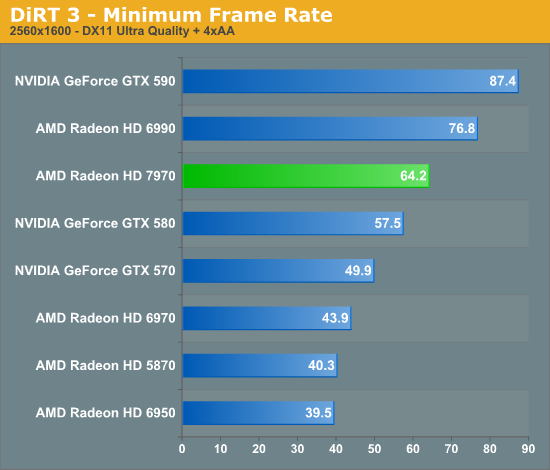
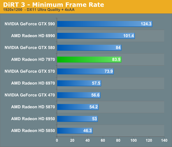
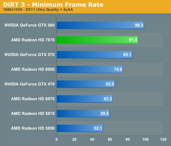
We’ve had a number of requests for more minimum framerates throughout the years, so we’re also going to include the minimum framerates for DiRT 3 as the minimums have proven to be reliably consistent in our benchmarks.
Given that the 7970 was already seeing a smaller than typical lead over the GTX 580, it’s not wholly surprising to see that it fares a bit worse when it comes to minimums. At 2560 its minimum framerate of 64.2fps means that the 7970 will deliver smooth performance every last moment, but at the same time this is only 11% better than the GTX 580. At 1920 this becomes a dead heat between the two cards. Meanwhile compared to the 6970 the 7970 is always about 45% ahead.
Total War: Shogun 2
One of our goals with this iteration of our benchmark suite was to throw in some additional non-FPS games, so we’re broadening our horizons a bit by adding in Total War: Shogun 2. Shogun 2 is the latest installment of the long-running Total War series of turn based strategy games, and alongside Civilization V is notable for just how many units it can put on a screen at once. As it also turns out, it’s the single most punishing game in our benchmark suite.
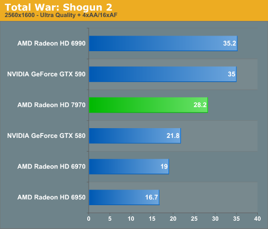
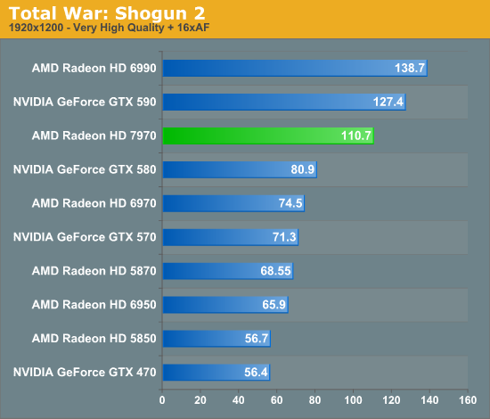
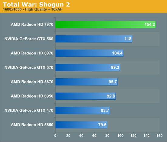
When deciding on what settings to use with Shogun, it required a bit more creativity on our part. 2560 is a true moonshot; everything is turned on, and it takes a minimum of 1.5GB of VRAM to run the game at this resolution. Accordingly performance is rather dismal, though as this is a TBS 30fps isn’t quite as critical as it is in other games. In any case the 7970 comes the closest to hitting 30fps, coming in just shy at 28.2fps, which is 29% ahead of the GTX 580 and 48% ahead of the 6970.
Meanwhile for 1920 we turned Shogun’s settings down to Very High, and yet we still had to disable MSAA to make it work with 1GB cards (did we mention that Shogun loves VRAM?). At these lower settings performance rockets up, and at the same time so does the 7970’s lead over the GTX 580. Here it’s 36% ahead of the GTX 580, which will be the greatest lead among all of our gaming benchmarks. As for the 7970 compared to the 6970, it’s still 48% of the 6970 showing us just how similar these video cards are at times.
Finally at 1680 the overall performance goes up yet again, but the 7970’s lead remains. It’s ahead of the GTX 580 by 30%, and 48% ahead of the 6970.
Batman: Arkham City
After a rocky launch last month, Rocksteady finally got their DirectX 11 problems sorted out for Batman: Arkham City earlier this month. Batman: Arkham City is loosely based on Unreal Engine 3, while the DirectX 11 functionality was apparently developed in-house. With the addition of these features Batman is far more a GPU demanding game than its predecessor was, particularly with tessellation cranked up to high.
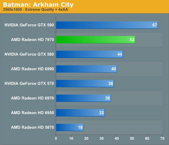
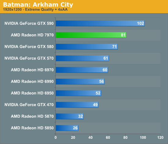
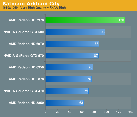
At Extreme settings Batman is quite daunting for our entire GPU lineup at 2560. Nothing except the GTX 590 can crack 60fps, though the 7970 begins to come close at 52fps. Relative to NVIDIA’s lineup Batman ends up being one of the weaker games for the 7970, with the 7970 only taking an 18% lead over the GTX 580 at 2560. As for the 6970, the 7970 has another very strong showing opposite AMD’s previous generation, beating the 6970 by 44%.
At 1920 we’re still using Extreme settings and the story is much the same, though the 7970’s lead drops a bit more. Against the GTX 580 it’s now only 14% faster, and against the 6970 it’s 35% faster. Things do eventually pick up at 1680 when we back off to Very High settings and stop using MSAA, at which point the 7970 takes a surprising 32% lead over the GTX 580 while the lead over the 6970 jumps back up to 47%.
Looking at all of our cards it’s really the 5870 that tells the whole story. Tessellation plays a large factor in Batman’s performance, and as a result the partially tessellation-constrained 5870 absolutely struggles even at 1920. Consequently this is further proof that AMD was able to get a great deal of additional performance out of their geometry engines even with the 2 tringle/clock limit.
Portal 2
Portal 2 continues the long and proud tradition of Valve’s in-house Source engine. While Source continues to be a DX9 engine, Valve has continued to upgrade it over the years to improve its quality, and combined with their choice of style you’d have a hard time telling it’s over 7 years old at this point. Consequently Portal 2’s performance does get rather high on high-end cards, but we have ways of fixing that…
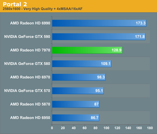
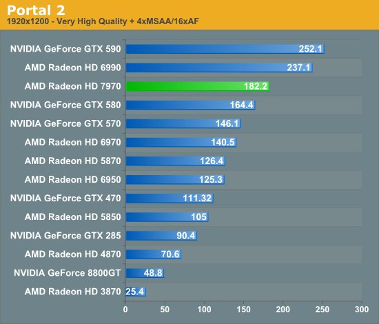
Given Portal 2’s wide range of performance it’s possible to at least somewhat bog it down on the GPU side without any special tricks thanks to its heavier use of shaders than in past Valve titles. Given a fast enough card I believe we could hit the 300fps internal Source framerate cap on our testbed, but thankfully at 2560 we’re nowhere close. In any case at 2560 the 7970 is well into the stratosphere, delivering 128.9fps, which is 18% better than the GTX 580. Meanwhile at 1920 as with so many other benchmarks that lead shrinks, this time down to 11%. Meanwhile the 7970 enjoys a smaller lead over the 6970, beating it by only around 30% at either resolution.
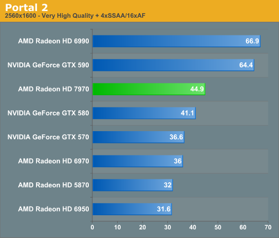
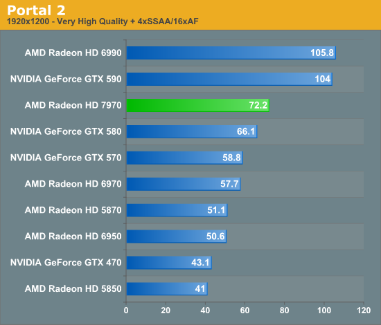
The great thing about the Source engine is that it’s well studied, and by utilizing DirectX9 it’s open to a few more image quality enhancements than DX10+ games. We’ve always wanted to have a standard benchmark with more anti-aliasing than just MSAA, and Portal is the perfect candidate. So for the second part of this test, we’ve turned on Super Sample Anti-Aliasing (SSAA) through NVIDIA and AMD’s driver control panels. With SSAA the entire scene gets anti-aliased, going beyond just removing the jaggies at polygon edges and removing all signs of shader aliasing too, making Portal 2 a very good looking game.
As expected, SSAA makes the performance of everything tank. At 2560 the 7970 is well below 60fps, and every other single-GPU card is slower yet. Once we get down to 1920 performance finally reaches a point where it’s playable, as the 7970 reaches 72.2fps.
Compared to its competition, it’s interesting to note that we appear to have hit an entirely different set of bottlenecks by using SSAA. The 7970 leads the GTX 580 by 9% at both resolutions while it leads the 6970 by 25% under the same conditions. We believe that at this point we’re seeing the limitations of ROP performance, which would explain why the 7970’s lead diminishes versus both the GTX 580 and 6970. The additional bandwidth the 7970’s design affords the ROPs can only go so far until it once again becomes a matter of pixel pushing power.
Battlefield 3
Its popularity aside, Battlefield 3 may be the most interesting game in our benchmark suite for a single reason: it’s the first AAA DX10+ game. It’s been 5 years since the launch of the first DX10 GPUs, and 3 whole process node shrinks later we’re finally to the point where games are using DX10’s functionality as a baseline rather than an addition. Not surprisingly BF3 is one of the best looking games in our suite, but as with past Battlefield games that beauty comes with a high performance cost
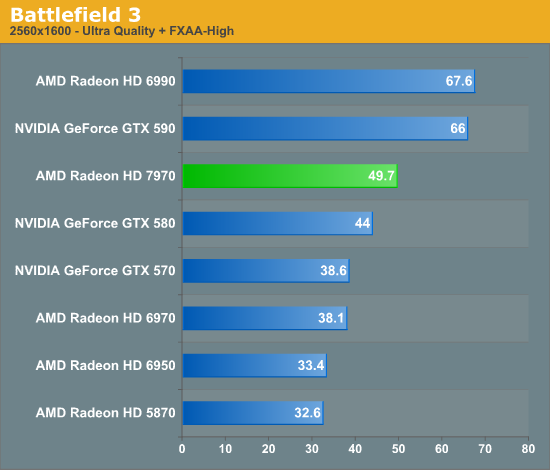
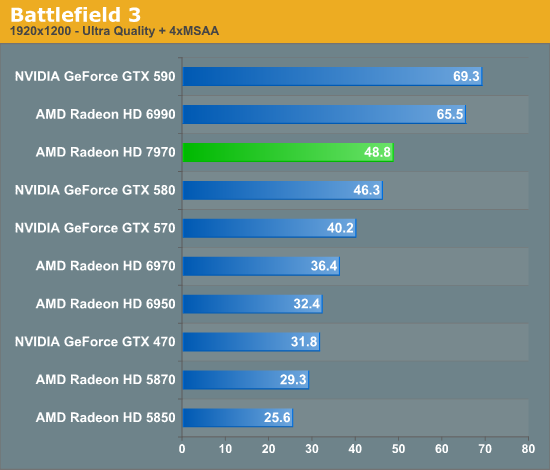
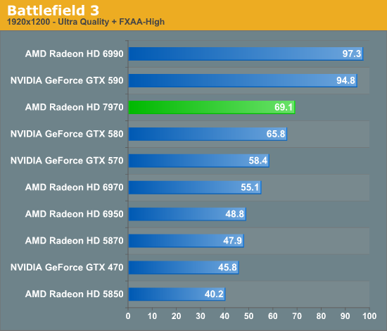
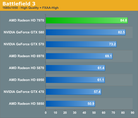
How to benchmark BF3 is a point of great contention. Our preference is to always stick to the scientific method, which means our tests need to be perfectly repeatable or very, very close. For that reason we’re using an on-rails section of the single player game, Thunder Run, to do our testing. This isn’t the most strenuous part of Battlefield 3 – multiplayer can get much worse – but it’s the most consistent part of the game. In general we’ve found that minimum framerates in multiplayer are about half of the average framerate in Thunder Run, so it’s important to frame your expectations accordingly.
With that out of the way, Battlefield 3 ends up being one of the worst games for the 7970 from a competitive standpoint. It always maintains a lead over the GTX 580, but the greatest lead is only 13% at 2560 without any MSAA, and everywhere else it’s 3-5%. Of course it goes without saying that realistically BF3 is only playable at 1920 (no MSAA) and below on any of the single-GPU cards in this lineup, so unfortunately for AMD it’s the 5% number that’s the most relevant.
Meanwhile compared to the 6970, the 7970’s performance gains are also a bit below average. 2560 and 1920 with MSAA are quite good at 30% and 34% respectively, but at 1920 without MSAA that’s only a 25% gain, which is one of the smaller gaps between the two cards throughout our entire test suite.
The big question of course is why are we only seeing such a limited lead from the 7970 here? BF3 implements a wide array of technologies so it’s hard to say for sure, but there is one thing we know they implement in the engine that only NVIDIA can use: Driver Command Lists, the same “secret sauce” that boosted NVIDIA’s Civilization V performance by so much last year. So it may be that NVIDIA’s DCL support is helping their performance here in BF3, much like it was in Civ V.
But in any case, this is probably the only benchmark that’s really under delivered for the 7970. 5% is still a performance improvement (and we’ll take it any day of the week), but this silences any reasonable hope of being able to use 1920 at Ultra settings with MSAA on a single-GPU card for the time being.
Starcraft II
Our next game is Starcraft II, Blizzard’s 2010 RTS megahit. Much like Portal 2 it’s a DX9 game designed to run on a wide range of hardware so performance is quite peppy with most high-end cards, but it can still challenge a GPU when it needs to.
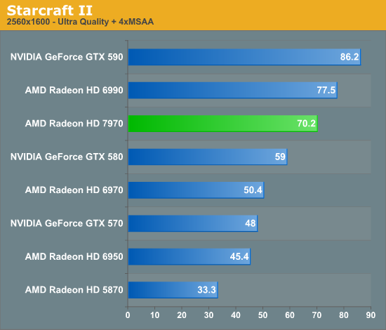
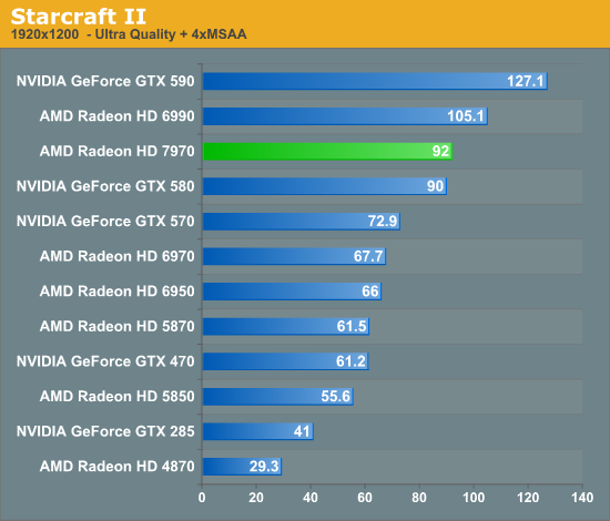
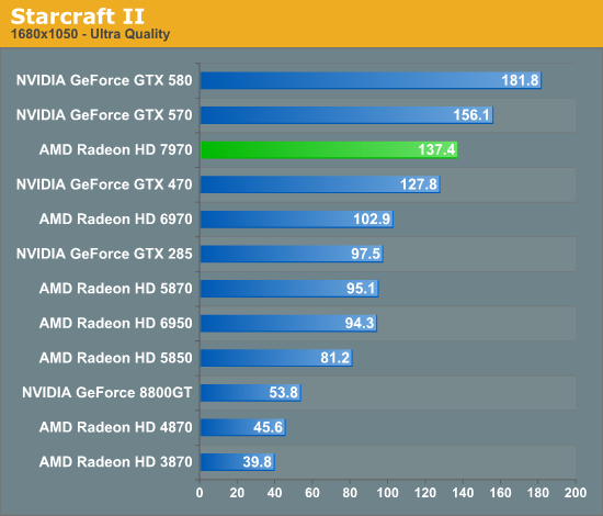
For 2560 and 1920 we’re using 4x MSAA, which must be forced through the driver control panel as Starcraft II does not natively support anti-aliasing. As is often the case with forced MSAA the resulting performance hit is rather high, which is why SC2 can still tax our high-end GPUs.
Starting at 2560, things are looking good for the 7960. At 70.2fps it takes a 19% lead over the GTX 580, and is the only single-GPU card to crack 60fps at that resolution. Against the 6970 it also looks quite good, with a lead of just under 40%.
But when we drop down to 1920, the 7970’s tendency for its lead to drop with the resolution takes full force. Here the 7970 is only 2% ahead of the GTX 580, and looking at 1680 (without MSAA) has the 7970 being outright outgassed by the older GTX 580 by nearly 33%. Interestingly enough however we don’t see the same thing happen against AMD’s own cards, as the 7970 remains ahead of the 6970 by about 35%.
While it’s primarily 1920 and 2560 we’re interested in, it’s still worth pondering on 1680 for a moment. Given the consistent performance of the 7970 versus the 6970, it looks like we’re not simply seeing architectural strengths and weaknesses here. AMD simply cannot hit the high framerates of the GTX 580 here, and at this point we have to suspect that unless AMD is somehow ROP-bound, that we’re looking at a driver limitation of some kind that starts to particularly manifest itself at 1920 and below.
In any case while Starcraft II is not a particularly strong game for the 7970, at the very least the raw performance is there. The performance differences are largely academic as the 7970 is more than capable of powering through even 2560. As such if the 7970 is going to struggle to beat the GTX 580 at any game, this is one of the less meaningful games to struggle at.
Civilization V
Our final game, Civilization 5, gives us an interesting look at things that other RTSes cannot match, with a much weaker focus on shading in the game world, and a much greater focus on creating the geometry needed to bring such a world to life. In doing so it uses a slew of DirectX 11 technologies, including tessellation for said geometry, driver command lists for reducing CPU overhead, and compute shaders for on-the-fly texture decompression.
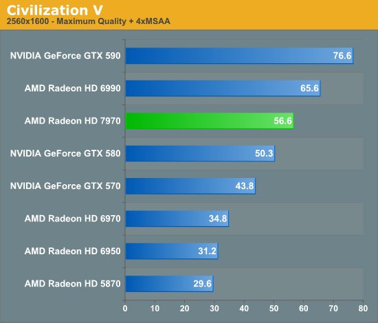
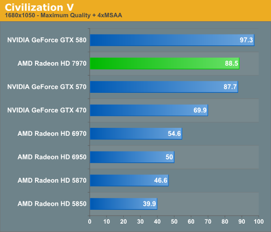
Because of the fact that Civilization V uses driver command lists, we were originally not going to include it in this benchmark suite as a gaming benchmark. If it were solely a DCL test it would do a good job highlighting the fact that AMD doesn’t currently support the feature, but a poor job of actually explaining any hardware/architectural differences. It was only after we saw AMD’s reviewer’s guide that we decided to go ahead and include it, because quite frankly we didn’t believe the numbers AMD had published.
With the GTX 580 and the 6970, the 6970 routinely lost to the GTX 580 by large margins. We had long assumed this was solely due to NVIDIA’s inclusion of DCLs, as we’ve seen a moderate single-GPU performance deficit and equally moderate multi-GPU lead for AMD melt away when NVIDIA added DCL support. The 7970 required that we rethink this.
If Civilization V was solely a DCL test, then our 2560 results would be impossible – the 7970 is winning by 12% in a game NVIDIA previous won by a massive margin. NVIDIA only regains their lead at 1680, which at this resolution we’re not nearly as likely to be GPU-bound.
So what changed? AMD has yet to spill the beans, but short of a secret DCL implementation for just CivV we have to look elsewhere. Next to DCL CivV’s other killer feature is its use of compute shaders, and GCN is a compute architecture. To that extent we believe at this point that while AMD is still facing some kind of DCL bottleneck, they have completely opened the floodgates on whatever compute shader bottleneck was standing in their way before. This is particularly evident when comparing the 7970 to the 6970, where the 7970 enjoys a consistent 62% performance advantage. It’s simply an incredible turnabout to see the 7970 do so well when the 6970 did so poorly.
Of course if this performance boost really was all about compute shaders, it raises a particularly exciting question: just how much higher could AMD go if they had DCLs? Hopefully one day that’s an answer we get to find out.
Compute: The Real Reason for GCN
Moving on from our game tests we’ve now reached the compute benchmark segment of our review. While the gaming performance of the 7970 will have the most immediate ramifications for AMD and the product, it is the compute performance that I believe is the more important metric in the long run. GCN is both a gaming and a compute architecture, and while its gaming pedigree is well defined its real-world compute capabilities still need to be exposed.
With that said, we’re going to open up this section with a rather straightforward statement: the current selection of compute applications for AMD GPUs is extremely poor. This is especially true for anything that would be suitable as a benchmark. Perhaps this is because developers ignored Evergreen and Northern Islands due to their low compute performance, or perhaps this is because developers still haven’t warmed up to OpenCL, but here at the tail end of 2011 there just aren’t very many applications that can make meaningful use of the pure compute capabilities of AMD’s GPUs.
Aggravating this some is that of the applications that can use AMD’s compute capabilities, some of the most popular ones among them have been hand-tuned for AMD’s previous architectures to the point that they simply will not run on Tahiti right now. Folding@Home, FLACC, and a few other candidates we looked into for use as compute benchmarks all fall under this umbrella, and as a result we only have a limited toolset to work with for proving the compute performance of GCN.
So with that out of the way, let’s get started.
Since we just ended with Civilization V as a gaming benchmark, let’s start with Civilization V as a compute benchmark. We’ve seen Civilization V’s performance skyrocket on 7970 and we’ve theorized that it’s due to improvements in compute shader performance, and now we have a chance to prove it.
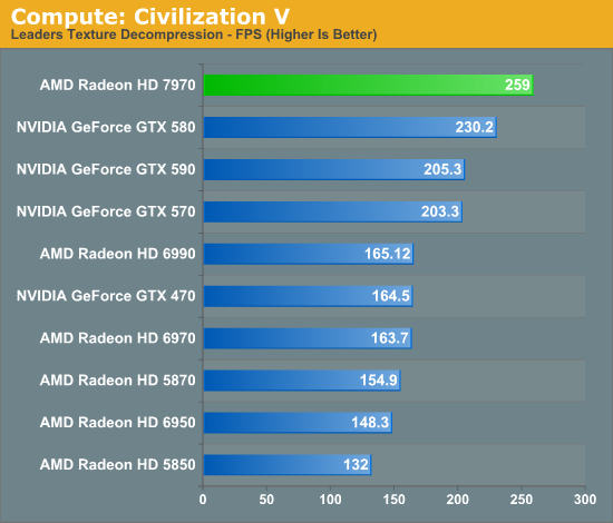
And there’s our proof. Compared to the 6970, the 7970’s performance on this benchmark has jumped up by 58%, and even the previously leading GTX 580 is now beneath the 7970 by 12%. GCN’s compute ambitions are clearly paying off, and in the case of Civilization V it’s even enough to dethrone NVIDIA entirely. If you’re AMD there’s not much more you can ask for.
Our next benchmark is SmallLuxGPU, the GPU ray tracing branch of the open source LuxRender renderer. We’re now using a development build from the version 2.0 branch, and we’ve moved on to a more complex scene that hopefully will provide a greater challenge to our GPUs.
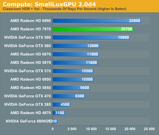
Again the 7970 does incredibly well here compared to AMD’s past architectures. AMD already did rather well here even with the limited compute performance of their VLIW4 architecture, and with GCN AMD once again puts their old architectures to shame, and puts NVIDIA to shame too in the process. Among single-GPU cards the GTX 580 is the closest competitor and even then the 7970 leads it by 72%. The story is much the same for the 7970 versus the 6970, where the 7970 leads by 74%. If AMD can continue to deliver on performance gains like these, the GCN is going to be a formidable force in the HPC market when it eventually makes its way there.
For our next benchmark we’re once again looking at compute shader performance, this time through the Fluid simulation sample in the DirectX SDK. This program simulates the motion and interactions of a 16k particle fluid using a compute shader, with a choice of several different algorithms. In this case we’re using two of them: a highly optimized grid search that Microsoft based on an earlier CUDA implementation, and an (O)n^2 nearest neighbor method that is optimized by using shared memory to cache data.
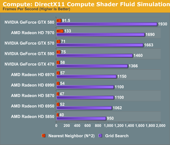
There are many things we can gather from this data, but let’s address the most important conclusions first. Regardless of the algorithm used, AMD’s VLIW4 and VLIW5 architectures had relatively poor performance in this simulation; NVIDIA meanwhile has strong performance with the grid search algorithm, but more limited performance with the shared memory algorithm. 7970 consequently manages to blow away the 6970 in all cases, and while it can’t beat the GTX 580 at the grid search algorithm it is 45% faster than the GTX 580 with the shared memory algorithm.
With GCN AMD put a lot of effort into compute performance, not only with respect to their shader/compute hardware, but with the caches and shared memory to feed that hardware. I don’t believe we have enough data to say anything definitive about how Tahiti/GCN’s cache compares to Fermi’s cache, this benchmark does raise the possibility that GCN cache design is better suited for less than optimal brute force algorithms. In which case what this means for AMD could be huge, as it could open up new HPC market opportunities for them that NVIDIA could never access, and certainly it could help AMD steal market share from NVIDIA.
Moving on to our final two benchmarks, we’ve gone spelunking through AMD’s OpenCL archive to dig up a couple more compute scenarios to use to evaluate GCN. The first of these is AESEncryptDecrypt, an OpenCL AES encryption routine that AES encrypts/decrypts an 8K x 8K pixel square image file. The results of this benchmark are the average time to encrypt the image over a number of iterations of the AES cypher.
We went into the AMD OpenCL sample archives knowing that the projects in it were likely already well suited for AMD’s previous architectures, and there is definitely a degree of that in our results. The 6970 already performs decently in this benchmark and ultimately the GTX 580 is the top competitor. However the 7970 still manages to improve on the 6970 by a sizable degree, and accomplishes this encryption task in only 65% the time. Meanwhile compared to the GTX 580 it trails by roughly 12%, which shows that if nothing else Fermi and GCN are going to have their own architectural strengths and weaknesses, although there’s obviously some room for improvement.
One interesting fact we gathered from this compute benchmark is that it benefitted from the increase in bandwidth offered by PCI Express 3.0. With PCIe 3.0 the 7970 improves by about 10%, showcasing just how important transport bandwidth is for some compute tasks. Ultimately we’ll reach a point where even games will be able to take full advantage of PCIe 3.0, but for right now it’s the compute uses that will benefit the most.
Our final benchmark also comes from the AMD OpenCL archives, and it’s a variant of the Monte Carlo method implemented in OpenCL. Here we’re timing how long it takes to execute a 400 step simulation.
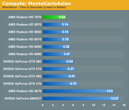
For our final benchmark the 7970 once again takes the lead. The rest of the Radeon pack is close behind so GCN isn’t providing an immense benefit here, but AMD still improves upon the 6970 by 14%. Meanwhile the lead over the GTX 580 is larger at 33%.
Ultimately from these benchmarks it’s clear that AMD is capable of delivering on at least some of the theoretical potential for compute performance that GCN brings to the table. Not unlike gaming performance this is often going to depend on the task at hand, but the performance here proves that in the right scenario Tahiti is a very capable compute GPU. Will it be enough to make a run at NVIDIA’s domination with Tesla? At this point it’s too early to tell, but the potential is there, which is much more than we could say about VLIW4.
Theoreticals & Tessellation
From a rendering perspective one of the most interesting things AMD did with Tahiti was what they didn’t do: they didn’t add more ROPs, they didn’t add more geometry engines. And yet based on our game performance they’ve clearly improved on their performance in those situations by making more efficient use of the hardware they do have.
So we wanted to take a quick look at synthetic performance to see what these tools had to say about AMD’s changes. We’ve included the numbers for every other GPU in our lineup as a reference point, but we would strongly suggest against reading into them too much. AMD versus AMD is sometimes relevant to real world performance; AMD versus NVIDIA rarely is.
We’ll start with 3DMark Vantage and its color fill test. This is basically a ROP test that attempts to have a GPU’s ROPs blend as many pixels as it can. Theoretically AMD can do 32 color operations per clock on Tahiti, which at 925MHz for 7970 means the theoretical limit is 29.6Gpix/sec; not that any architecture is ever that efficient. In practice 7970 hits 13.33Gpix/sec, which is still well short of the theoretical maximum, but pay close attention to 7970’s performance relative to 6970. Even with the same number of ROPs and a similar theoretical performance limit (29.6 vs 28.16), 7970 is pushing 51% more pixels than 6970 is.
In designing Tahiti AMD said that they didn’t need more ROPs they just needed more efficient ROPs, and it looks like they’ve delivered on this. It’s not clear whether this is the limit for efficiency or if AMD can squeeze more out of their ROPs in future designs, but this definitely helps to prove that there’s more to graphics rendering than a large number of functional units.
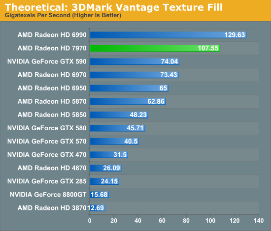
Our other 3DMark synthetic benchmark is the 3DMark Vantage Texture Blend test, which measures how quickly a GPU can blend multiple FP16 textures. This is more synthetic than most tests because FP16 textures aren’t widely used, but it’s a consistent benchmark.
The theoretical performance improvement from 6970 to 7970 is 40% - 33% more texture units operating at a 5% higher clockspeed. In practice the 7970 exceeds that improvement by increasing texture performance by 46%, meaning the 7970 has benefitted from more than the increase in texture units. Most likely the new cache architecture has further improved the efficiency of the texture units, although the 3DMark texture set is not particularly large.
Moving on, we also wanted to take a look at tessellation. AMD did not increase the theoretical geometry performance of Tahiti as compared to Cayman – both top out at 2 triangles per clock – but AMD has put a lot of effort into improving the efficiency of Tahiti’s geometry units as we’ve seen reflected in our game benchmarks.
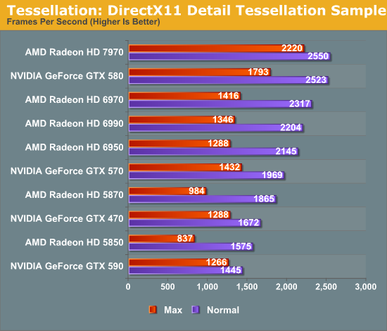
Our first tessellation benchmark is the traditional Detail Tessellation sample program from the DirectX SDK. Here we’re looking at tessellation performance as a product of the framerate, testing at tessellation factors 7 (normal) and 15 (max). Traditionally this is a test that has been rather balanced at normal tessellation levels, while NVIDIA cards with their superior geometry throughput have been the top performers at maximum tessellation levels. So it’s all the more interesting when we’ve seen the tables turned; the 7970 is merely competitive with the GTX 580 at normal tessellation levels, but now it’s ahead of the GTX 580 by 24%. More significantly however the 7970 is ahead of the 6970 by 57%.
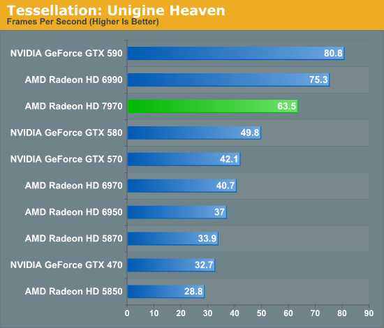
Our second tessellation benchmark is Unigine Heaven, a benchmark that straddles the line between a synthetic benchmark and a real-world benchmark, as the engine is licensed but no notable DX11 games have been produced using it yet. In any case the Heaven benchmark is notable for its heavy use of tessellation, which means it’s largely a proxy test for tessellation performance.
As with the Detail Tessellation sample program, Heaven shows significant gains for the 7970 versus the 6970, with the 7970 leading by 56%. Meanwhile it leads the GTX 580 by 27%, which is actually slightly better than what we saw under the more “pure” Detail Tessellation sample. Between these two benchmarks it’s clear that AMD’s tessellation efficiency improvements are quite real, and that with Tahiti AMD can deliver much better tessellation performance than Cayman even at virtually the same theoretical triangle throughput rate.
Of course one has to wonder what NVIDIA will have in store for Kepler next year. Their current Fermi design seems to scale well with additional geometry units, but if Tahiti is anything to go by, there’s a great deal to be gained just by focusing on efficiency. NVIDIA has prided themselves on their geometry performance since before GF100 even shipped, so it will be interesting if they have anything in store to hold on to that distinction.
Power, Temperature, & Noise
As always, we wrap up our look at a new video card with a look at the physical performance attributes: power consumption, temperatures, and noise. With new process nodes being the lifeblood of the GPU industry, each new process gives GPU manufacturers a chance to move their product along a continuum; do they take advantage of a power consumption reduction for the same performance level, a performance increase for the same power consumption, or something in between? In AMD’s case they’ve chosen to try to maximize performance within Cayman’s power budget, which means power, temperature, and noise should be similar to what we’ve seen with 6970, cooler improvements not withstanding.
Before we get into the charts, it’s worth noting right now that we don’t have a good idea of what 7970’s operational voltage is, as we don’t have any tools that can read 7970’s VRMs. We believe it’s close to Cayman’s, but this is something that will require confirmation in the future.
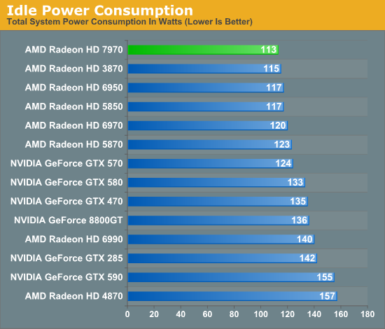
Starting as always with idle power, we can immediately see the benefits of the work AMD has put into idle power usage with Southern Islands. AMD has been working hard to reduce idle power consumption since the 4870 and at this point they’ve finally beaten even the 3870, which was a relatively small GPU using GDDR3 RAM. AMD’s official typical idle TDP here is 15W, and we have little doubt they’re going to continue to whittle that number down on future generations.
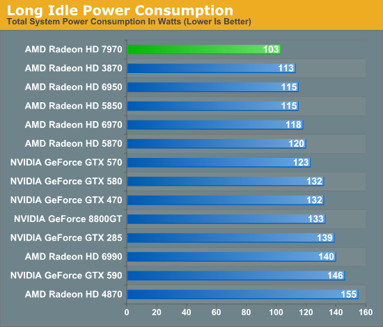
While we’re looking at idle power, we also wanted to take a look at AMD’s “long idle” scenario, where a blanked display or being slave GPU in a multi-GPU setup gives a GPU the opportunity to go into a deeper sleep state as it’s not needed for any work. Through ZeroCore Power AMD is able to shut off virtually every aspect of Tahiti when in a long idle state, allowing AMD to reduce the power consumption of 7970 to under 3W. Meanwhile for every other card there’s a very slight gain to be had in long idle because the GPU can power down all of its display transmitters, but it’s not nearly as effective as shutting down the entire GPU, which is why 7970 has a 10W advantage at the wall versus the next closest GPU.
As we said earlier in our look at ZeroCore Power technology, while the numbers are impressive enough, for the desktop the real use will be in multi-GPU systems as slave GPUs can be put in a ZCP state even while the master GPU is awake and working, significantly reducing idle power and noise in multi-GPU systems.
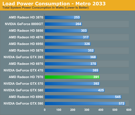
Moving on to our load power tests, based on our testing we have swapped out Crysis for Metro 2033 in this iteration of our benchmark suite as Metro 2033 was proving to be a bit more strenuous on our GPUs and is the only game to ever trigger PowerTune on the 6970.
Looking at Metro it’s clear that the smaller fabrication process for 6970 has allowed AMD to achieve a lower power consumption level relative to their gaming performance – the 7970 leads the GTX 580 by 20-30% in performance while consuming 34W less at the wall. At the same time this test calls into question AMD’s power targets. We’re clearly drawing more power than the 6970 – 21W more to be precise – and while this could be explained by CPU power consumption I’m not convinced that’s the case.
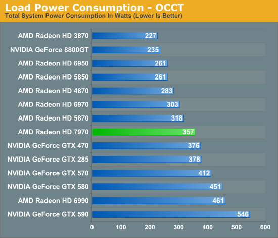
As for our pathological power consumption test we’ve moved on to OCCT, which at this point in time escapes NVIDIA’s throttling mechanism and in spite of the presence of PowerTune still manages to be a hardware workload on AMD’s GPUs than FurMark. OCCT backs up our earlier data from Metro that 7970 draws more power than 6970 even with the similar power targets. We’re drawing 50W more at the wall, which on paper at least would put 7970’s power consumption closer to 280W if AMD’s original 250W target for 6970 is still correct. If all of this is correct, then it calls into doubt AMD’s published power targets, as it looks like AMD has made a power/performance tradeoff with 7970 by trading slightly higher power consumption for what would be higher performance.
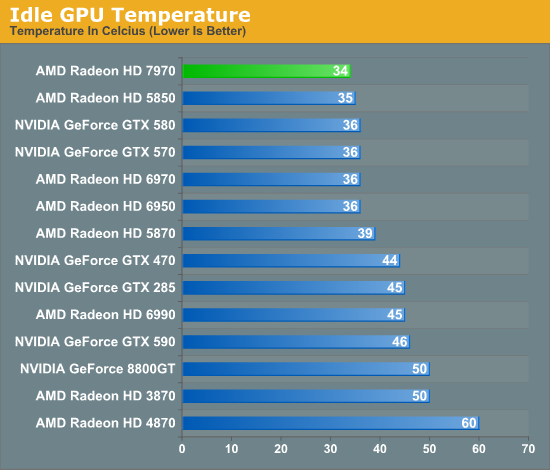
Up next is our look at idle temperatures. All of the last generation GPUs were highly competitive here and as a result it’s a tough crowd as there’s relatively little room to further reduce a GPU’s temperature. Nevertheless the 7970 manages to squeak by the competition, with a recorded idle temperature of 34C, 1C lower than the GTX 580 and 2C lower than the 6970.
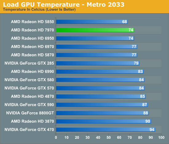
Moving on to temperatures under Metro, the results are quite surprising: the 7970 does really, really good here given its power consumption. At 74C the only cooler video cards are the 6850 and 5850, both of which are lower tier, lower power versions of higher end parts. Part of this can be traced back to AMD’s cooling optimizations such as moving back to a full slot exhaust vent, but I don’t believe that’s a full explanation. We’ll get back to this when we’re looking at noise.
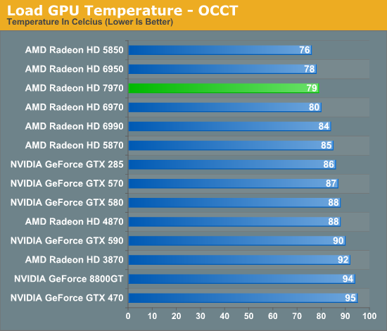
While the overall numbers are higher in OCCT, the relative rankings are unchanged from Metro. The only cooler cards in this lineup are the 6950 and 5850. Here the 7970 hits 79C, while the 6970 is slightly behind at 80C, and the GTX 500 series is in the upper 80s.
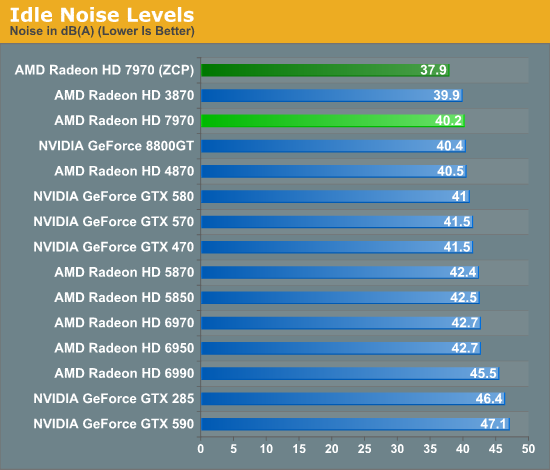
Last we have our look at noise, starting with idle noise. Much like our idle temperatures most single-GPU video cards tend to cluster together within 1dB, but the 7970 has managed to silence most of the rest of the pack, with a recorded noise level of 40.2dB. More impressive perhaps is the 7970 when in its Zero Core Power state. Because the fan turns off, the card is silent; 37.9dB(A) is the noise floor of our testbed.
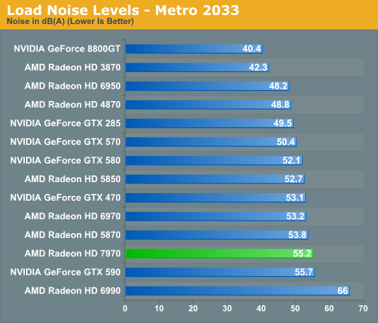
Moving on to our load noise measurements the full picture of the 7970’s cooling performance finally starts coming together. We’ve seen that the 7970 is a cool card, but is it a quiet card? The numbers say no. The 7970 is 3dB louder than the GTX 580 and 2dB louder than the 6970 even with its physical cooling improvements. Based on this combined with our temperature data it’s clear that AMD has targeted aggressive cooling over silence, whereas NVIDIA traditionally targets silence over aggressive cooling. When it comes to our testbed AMD has probably overdone it – we could easily exchange 10C for less noise – but with a wide range of computers in the world it’s hard to tell from a single testbed whether the cooling here is genuinely too aggressive for everyone, or if it’s the opposite. What isn’t in question is that the 7970 is going to be moderately loud, which coming from AMD is a surprising development.
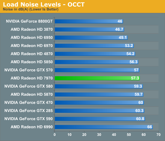
Once again with OCCT the numbers are higher, but the facts are largely the same. The 7970 is now quieter than the GTX 580 due to PowerTune, but it’s now 4dB louder than the 6970. Unlike Metro 57.3dB of noise is in the middle of the pack, but it stands to reason that AMD could have been a bit less aggressive on their fan speeds and made a quieter card as a result.
Final Words
The launch of the Radeon HD 7970 has presented us with a great deal of data and even more subjects to consider, so it’s difficult in the best of times to try to whittle this down to a single conclusion. Nevertheless, based on our testing I believe there are two distinct conclusions to be drawn: the case for gaming, and the case for computing.
Gaming
At the end of the day the 7970 is specifically targeted as a gaming workhorse. Regardless of any architecture changes, what’s important is how fast the card is, how much it costs, whether it works correctly, and what its physical attributes are like. With respect to all of these aspects AMD has made an acceptable card, but this is not a groundbreaking product like we’ve seen in the past.
The fact of the matter is that since 2008 we’ve become spoiled by AMD’s aggressive pricing. More than anything else the low prices of the Radeon HD 4870 and Radeon HD 5870 made those products superstars thanks to their performance for the price and their undercutting of NVIDIA’s competing cards. The Radeon HD 5870 was definitely fast, but at $379 it was a steal, which is part of the reason prices for it never stabilized at that low a level.
At the same time the 7970 is not the 5870. The 5870 relative to both NVIDIA and AMD’s previous generation video cards was faster on a percentage basis. It was more clearly a next-generation card, and DX11 only helped to seal the deal. Meanwhile if you look at straight averages the 7970 is only around 15-25% faster than the GTX 580 in our tests, with its advantage being highly game dependent. It always wins at 2560 and 1920, but there are some cases where it’s not much of a win. The 7970’s domination of the 6970 is more absolute, but then again the 6970 is a good $200 cheaper at this point in time.
Meanwhile the presence of previous generation dual-GPU cards will continue to muddle the picture a bit further. We remain as sheepish as ever on multi-GPU cards and believe a high performance single GPU card is still a better investment in most situations, but there’s no denying that the GTX 590 and Radeon HD 6990 are quite capable cards today if you can put up with the noise and the inherent issues with alternate frame rendering.
Ultimately the past few years have seen AMD make great technical progress, but on the business side of things it’s NVIDIA that has made all the money. GCN will help AMD here by improving their professional product line, but the other part of that equation is for AMD to stop selling their cards for so little when they don’t have to. And this is what we’re seeing with the Radeon HD 7970. AMD has chosen to price the 7970 like a current generation card – it’s priced relative to a 3GB GTX 580 – and that’s a fair metric. What it isn’t is groundbreaking in any sense.
So at the end of the day AMD has once again retaken the performance crown for single-GPU cards, bringing them back to a position they last held nearly 2 years ago with the 5870. To that AMD deserves kudos, and if you’re in the market for a $500+ video card the 7970 is clearly the card to get – it’s a bit more expensive than the GTX 580, but it’s reasonably faster and cooler all at once. However if you’ve been waiting for 28nm GPUs to bring about another rapid decrease in video card prices as we saw with the 5870, you’re going to be waiting a bit longer.
Compute
The Radeon HD 7970 may be a gaming product, but today was just as much a launch for AMD’s Graphics Core Next architecture as it was for their new single-GPU king. GCN is the biggest architecture overhaul for AMD since R600 in 2007, and it shows. AMD has laid out a clear plan to seriously break into the GPU computing market and GCN is the architecture that will take them there. This is their Fermi moment.
At this point I’m not comfortable speaking about the compute performance of GCN in absolutes, but based on our limited testing with the 7970 it’s clear the potential is there. At times it’s competitive with the Fermi-based GTX 580 and at other times it’s quite a bit faster. In the hands of experienced developers and given enough time to learn the quirks of GCN, I believe GCN will prove itself. It’s much too early to tell if it will be able to withstand the eventual arrival of NVIDIA’s Kepler, but certainly this is the best shot AMD has ever had.
Performance aside, it’s clear that AMD’s SIMD architecture will make GPU compute development for GCN much easier; of that there is no question. This is important as GCN isn’t just about HPC computing, it’s about fully embracing Fusion. AMD’s CPU plans are built upon GCN just as much as they’re built upon Bulldozer, and for GCN to deliver on its half of the heterogeneous computing aspect of Fusion it will need to be easy to program and it will need to perform well. It would appear AMD has the hardware to make the former happen, now time will tell if GCN Fusion can deliver on the latter.


